
The Hidden Costs of DIY Electronics: Why Components Fail
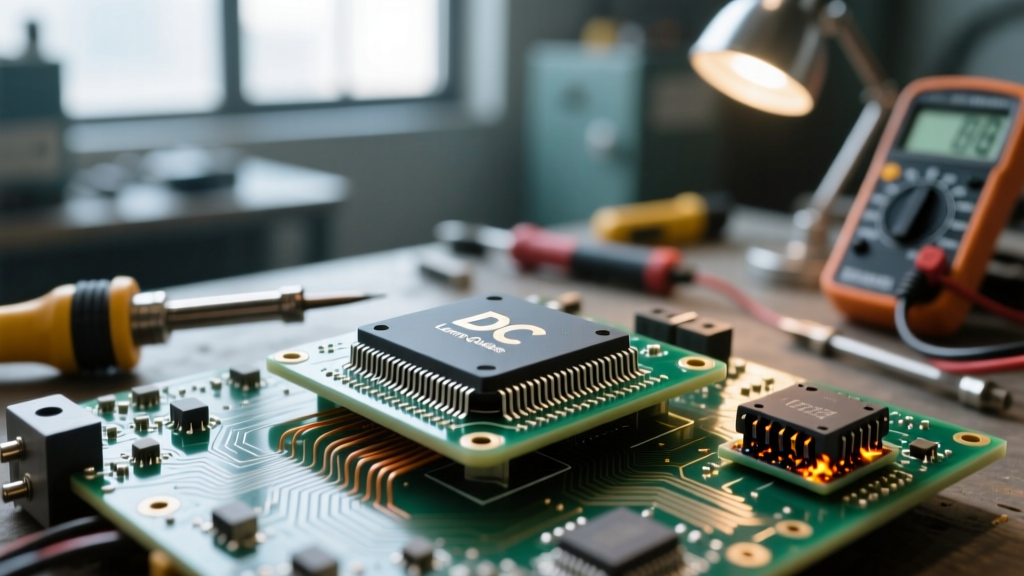
Building custom PCBs, programming microcontrollers, and assembling robotics kits are cornerstones of the DIY electronics hobby. However, as surface-mount components shrink and logic voltages drop to 1.8V or lower, the margin for error has vanished. Experiencing electronic components damage is practically a rite of passage for beginners, but for seasoned engineers, it represents a preventable loss of time and money. Frying a $15 STM32F4 microcontroller or a $45 TI DRV8825 motor driver usually comes down to three distinct physical mechanisms: thermal stress, electrical overstress (EOS), and electrostatic discharge (ESD).
In this guide, we break down the exact failure modes, the specific workbench protocols required to mitigate them, and how to troubleshoot a suspected dead IC using standard bench equipment.
The Big Three: Thermal, Electrical, and ESD Failures
1. Thermal Damage and the 'Popcorn' Effect
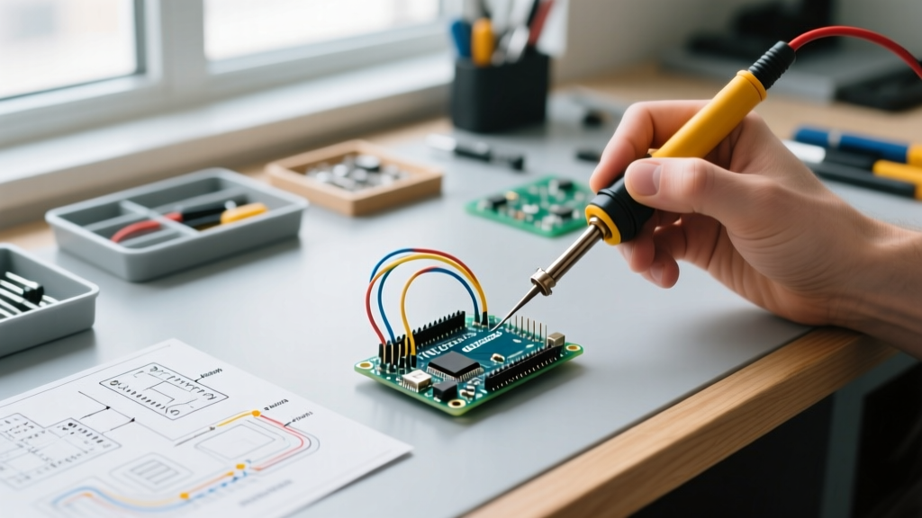
Thermal damage occurs when the heat applied during soldering exceeds the component's maximum junction temperature or dwell time. Modern lead-free solder alloys, like SAC305 (Tin/Silver/Copper), require higher iron temperatures—typically 340°C to 360°C—compared to legacy leaded solders. If you hold a standard chisel tip on a 0603 resistor pad for more than three seconds, the internal termination layers can delaminate.
More insidious is moisture-induced thermal damage. ICs like the ESP32-S3 are rated with a Moisture Sensitivity Level (MSL). An MSL 3 component can only be exposed to ambient room conditions (under 60% relative humidity) for 168 hours before reflow. If moisture penetrates the plastic package and you apply 350°C heat, the water instantly vaporizes, expanding and cracking the silicon die from the inside out—a phenomenon known as the 'popcorn effect.' To prevent this, store sensitive ICs in sealed ESD bags with desiccant, or bake them at 125°C for 4 hours before soldering.
2. Electrical Overstress (EOS) and Inductive Kickback
EOS is the application of voltage or current beyond the absolute maximum ratings of a device. The most common DIY culprit is inductive kickback. When you use an Arduino to switch a 12V relay via a transistor, the relay coil stores energy in its magnetic field. When the transistor turns off, the collapsing field generates a massive reverse voltage spike (often exceeding 100V). Without a flyback diode (like a 1N4004) wired in reverse bias across the coil, this spike instantly punches through the transistor's collector-emitter junction and can back-feed into the microcontroller's GPIO pin, permanently shorting the I/O bank.
Another frequent EOS scenario is logic-level mismatch. Driving a 3.3V sensor (like the BME280) directly from a 5V logic line without a level shifter (such as a BSS138 MOSFET-based bidirectional translator) will overstress the sensor's internal ESD protection diodes, leading to excessive current draw and eventual thermal runaway.
3. Electrostatic Discharge (ESD) and Gate Oxide Puncture
ESD is a rapid, high-voltage transfer of static charge. Walking across a synthetic carpet can generate up to 15,000V on the human body. While the current is low, the voltage is more than enough to puncture the nanometer-thin silicon dioxide gate layer of a MOSFET (like the popular IRF540N) or the input stage of a CMOS logic chip. According to Analog Devices, ESD damage often doesn't result in immediate catastrophic failure; instead, it creates a 'latent defect' where the component operates normally but degrades rapidly, failing weeks later under standard operating loads.
Failure Mode Matrix: Identifying the Culprit
Diagnosing the root cause of electronic components damage requires matching the physical symptoms to the stressor. Use this matrix to identify what killed your part.
| Failure Type | Visual Symptom | Multimeter Test (Diode Mode) | Primary Prevention Method |
|---|---|---|---|
| Thermal | Discolored PCB pads, cracked IC epoxy, lifted traces. | Erratic readings; bond wires may lift causing open circuits (OL). | Limit dwell time to <3s; use pre-heaters for large ground planes. |
| EOS | Burn marks, melted plastic, visible silicon cratering. | Dead short (0.00V) between VCC and GND, or I/O to GND. | Install flyback diodes, TVS diodes, and logic level shifters. |
| ESD | No visible damage; component looks pristine. | Leakage current present; forward voltage drops lower than spec. | Use grounded ESD mats, wrist straps, and ionizing fans. |
Essential Protection Gear for the 2026 DIY Workbench
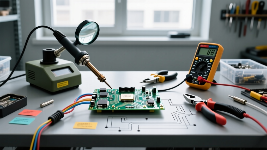
Upgrading your workbench to meet basic IPC standards for handling sensitive assemblies doesn't require a commercial budget. Here is a highly specific, cost-effective setup:
- ESD Wrist Strap: The Desco 09125 adjustable wrist strap (approx. $15) includes a built-in 1-megohm safety resistor. This limits current flow to safe levels if you accidentally touch a live mains voltage while grounded.
- Dissipative Mat: A 3M 4000 series two-layer rubber mat (approx. $110 for a 24x36 inch roll). The top layer is static-dissipative (10^6 to 10^8 ohms), slowing the discharge rate so it doesn't harm components, while the bottom layer is conductive to ground.
- Temperature-Controlled Station: Avoid cheap $30 unregulated irons. Invest in a Hakko FX-888D or a JBC CD-2BQE (ranging from $120 to $450). These stations use active thermocouple feedback in the tip to recover heat instantly, allowing you to solder at lower baseline temperatures (320°C) without cold joints.
- Tacky Flux: Chip Quik SMD4300AX10 (approx. $25 for 10cc). This no-clean, rosin-based flux lowers the surface tension of the solder, drastically reducing the time the iron needs to stay on the pad.
Step-by-Step PCB Rework Protocol to Avoid Heat Damage
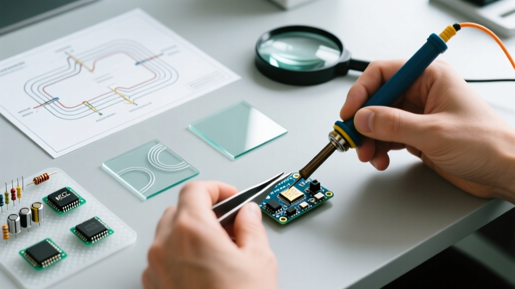
When replacing a damaged SOIC-8 or QFP package, improper heat application will destroy the replacement chip and lift the PCB pads. Follow this exact sequence:
- Pre-Heat the Board: If using a hot air rework station, set the bed or pre-heater to 120°C. This reduces the thermal gradient, meaning your hot air gun only needs to supply an additional 100°C to reach the 220°C reflow point, minimizing thermal shock to the fiberglass substrate.
- Apply Flux Generously: Coat all pins of the damaged IC with tacky flux. Flux is a chemical heat transfer medium; it ensures heat distributes evenly across all pins simultaneously.
- Add Leaded Solder: Mix 63/37 tin-lead solder onto the existing lead-free joints. This creates a eutectic alloy with a much lower melting point (183°C), making removal significantly faster and safer for the surrounding traces.
- Removal: Use a hot air gun set to 350°C with a medium airflow (approx. 40%). Heat in a continuous circular motion. Once the solder shines and liquefies, lift the IC straight up with tweezers. Never pry the chip while the solder is semi-solid; you will rip the copper pads off the board.
- Cleanup: Wick the remaining solder using a 2.0mm desoldering braid (like Goot Wick CP-2060) and a 340°C iron. Clean the area with 99% isopropyl alcohol and a lint-free swab.
Expert Troubleshooting: Did You Actually Fry It?
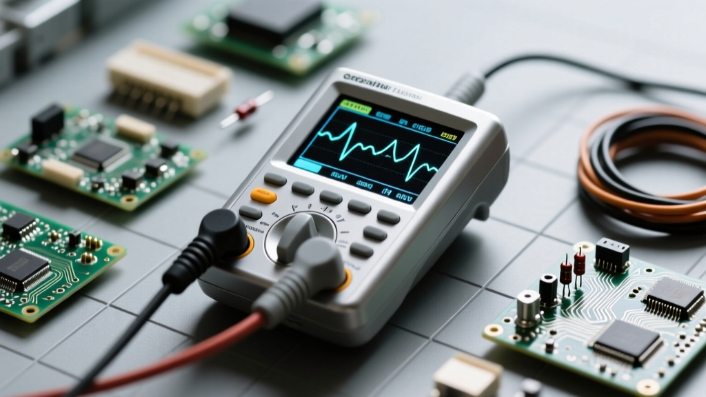
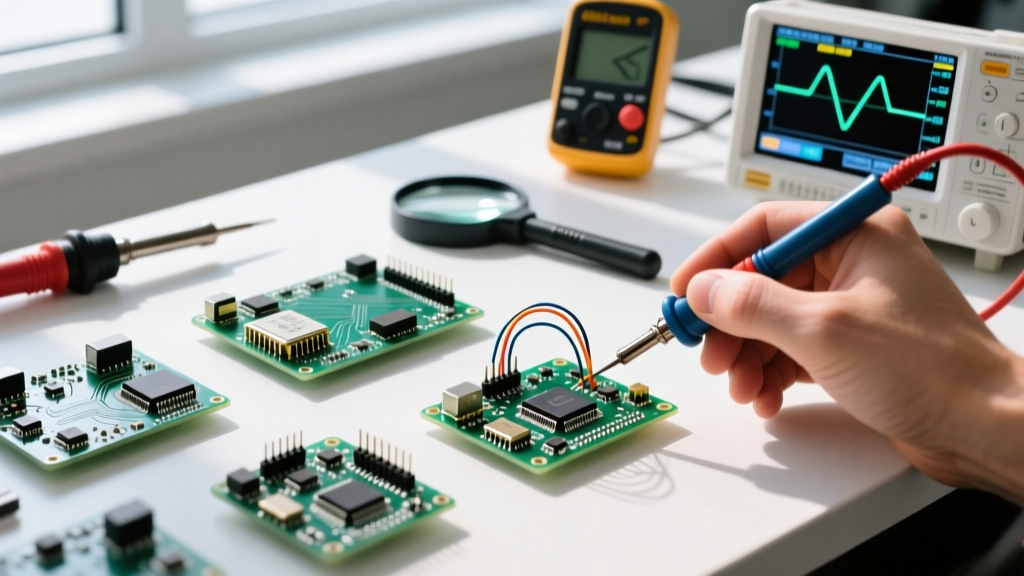
Before throwing a suspect microcontroller into the bin, verify the damage using the diode-test mode on a quality multimeter (such as the Fluke 87V or Brymen BM235). This technique, often called 'signature testing' or curve tracing, measures the forward voltage drop of the internal ESD protection diodes connected to every I/O pin.
Pro Tip: Set your multimeter to diode mode. Place the black (common) probe on the IC's ground pin. Touch the red probe to each I/O pin. A healthy CMOS microcontroller will typically read between 0.45V and 0.65V. If you read 'OL' (Open Loop), the internal bond wire has snapped (thermal or mechanical damage). If you read 0.00V to 0.10V, the ESD diode has been shorted to ground by an EOS event.
For a deeper dive into static safety protocols, the SparkFun ESD Tutorial provides excellent visual guides on setting up a grounded workspace. By respecting the physical limits of silicon, managing thermal gradients, and clamping inductive voltages, you can effectively eliminate electronic components damage from your DIY workflow, saving hundreds of dollars and countless hours of debugging.