
The Leap from Breadboard to Factory Floor
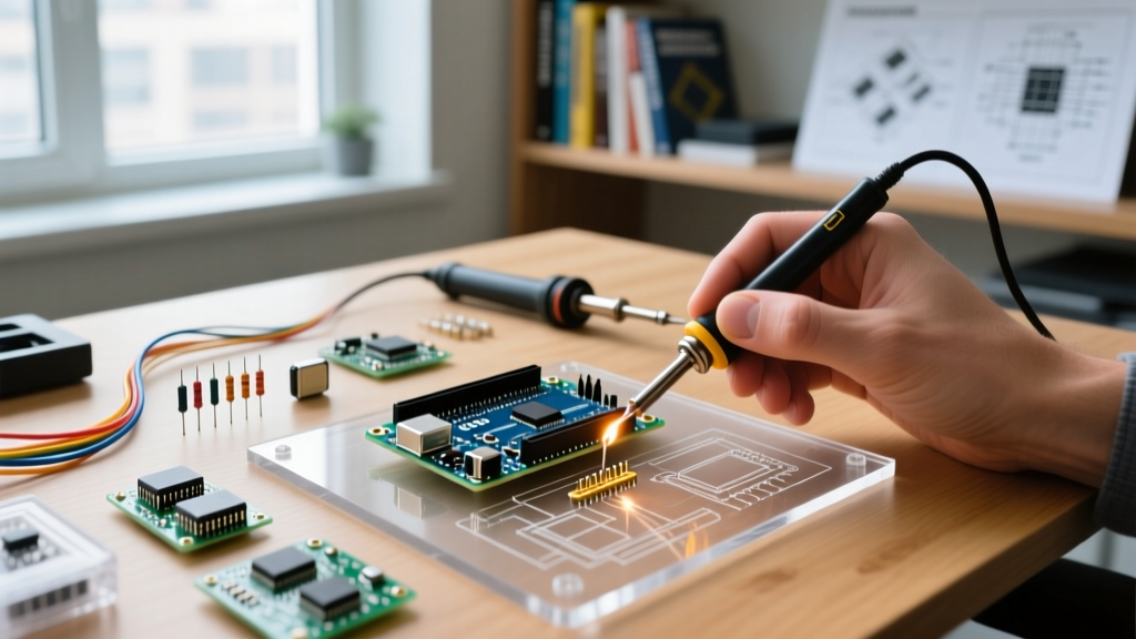
For most electronics hobbyists, the journey begins with a soldering iron, a breadboard, and off-the-shelf modules. But as your projects evolve into commercial products or complex custom hardware, you inevitably hit a wall: hand-soldering 500 boards with 0402 components and QFN ICs is physically impossible and economically unviable. This is where understanding electronic components manufacturing becomes your most valuable skill.
Transitioning from a DIY tinkerer to a hardware designer capable of managing small-batch Printed Circuit Board Assembly (PCBA) requires a structured skill-building path. In 2026, the barrier to entry for professional-grade manufacturing has never been lower, thanks to automated turnkey assembly services and AI-driven Design for Manufacturing (DFM) tools. However, the physics of solder, the strictness of IPC standards, and the realities of global supply chains remain unforgiving to the unprepared.
The 2026 Reality Check: According to the Surface Mount Technology Association (SMTA), over 65% of first-time PCBA failures in small-batch runs are traced back to poor BOM (Bill of Materials) formatting and incorrect component footprint design, not factory errors.
This guide outlines a four-phase skill-building path to master electronic components manufacturing, taking you from basic sourcing to full-scale quality control.
Phase 1: Professional Component Sourcing and Verification
The foundation of reliable manufacturing is authentic, traceable components. The gray market is flooded with counterfeit ICs and recycled capacitors that will fail during reflow or in the field.
Moving Beyond Marketplaces
While AliExpress and Amazon are fine for prototyping, manufacturing requires authorized distributors. You must build accounts with tier-one suppliers like Digi-Key Electronics, Mouser, or verified Asian equivalents like LCSC. These platforms guarantee the chain of custody directly from the original component manufacturer (OCM).
Understanding Moisture Sensitivity Levels (MSL)
One of the most overlooked skills in component manufacturing is managing Moisture Sensitivity Levels (MSL). ICs with plastic packages absorb ambient humidity. When exposed to 250°C reflow temperatures, the trapped water turns to steam, causing the 'popcorn effect'—micro-fractures inside the silicon package.
- MSL 1 & 2: Generally safe for standard turnkey assembly without special handling.
- MSL 3 to 6: Require strict dry-pack storage. If the humidity indicator card shows a breach, components must be baked at 125°C for 24 hours before reflow soldering.
Pro Tip: Always check the MSL rating on your BOM. If you are sourcing MSL 4 components from a distributor that doesn't use nitrogen-purged dry cabinets, you must instruct your PCBA house to bake the parts before assembly.
Phase 2: Design for Manufacturing (DFM) Mastery
A PCB that works on your desk might be unmanufacturable at scale. DFM is the practice of designing your board so that automated pick-and-place machines and reflow ovens can process it without defects. The IPC Standards (specifically IPC-2221 for design and IPC-A-610 for acceptability) are your bible here.
Critical DFM Metrics for 2026
To keep manufacturing costs low and yields high, adhere to these baseline specifications when designing in Altium, KiCad, or EasyEDA:
- Minimum Trace/Space: Stick to 0.15mm (6 mil) for standard boards. Dropping to 0.1mm (4 mil) increases fab costs by 15-20% and requires advanced etching.
- Via Annular Rings: Maintain at least a 0.15mm annular ring. Smaller rings risk drill breakout, causing open circuits.
- Component Placement: Align all polarized components (diodes, electrolytic capacitors) in the same direction. This allows the assembly house to optimize the pick-and-place feeder setup, reducing assembly time and cost.
- Fiducial Marks: Always include three global fiducial marks on the PCB panel and local fiducials near fine-pitch components (like BGAs or 0.4mm pitch QFPs). The vision systems on pick-and-place machines rely on these to align components with 0.01mm accuracy.
Phase 3: BOM Preparation and Turnkey PCBA
When you order turnkey assembly (where the factory sources parts and solders them), your BOM and CPL (Component Placement List) must be flawless. A single typo in a manufacturer part number (MPN) can result in the factory stuffing 10kΩ resistors where 1kΩ was intended.
The Perfect BOM Structure
Format your BOM as a clean CSV file with the following exact columns to ensure compatibility with automated quoting engines:
- Designator: (e.g., C1, C2, R14) - Must match the CPL exactly.
- Quantity: Number of identical parts per board.
- MPN (Manufacturer Part Number): The exact string from the datasheet (e.g., GRM155R71C104KA88D). Do not use internal SKUs.
- Manufacturer: (e.g., Murata, Texas Instruments).
- Value & Tolerance: (e.g., 100nF, 10%, 16V).
- Package/Footprint: (e.g., 0402, SOT-23-5).
Small-Batch PCBA Service Comparison
Choosing the right manufacturing partner depends on your volume, budget, and component complexity. Below is a comparison of leading small-batch turnkey services available in 2026:
| Service Provider | Best For | Base Setup Cost (Approx) | Component Sourcing | Min. Order |
|---|---|---|---|---|
| JLCPCB | Ultra-low cost, basic 0402/SOIC designs | $8.00 + Stencil ($15) | LCSC library (Limited Digi-Key integration) | 2 Boards |
| PCBWay | Complex BGAs, rigid-flex, advanced DFM support | $30.00 + Stencil ($25) | Global sourcing, Mouser/Digi-Key integration | 5 Boards |
| Seeed Fusion | IoT modules, rapid prototyping with testing | $25.00 + Stencil ($20) | Extensive global network, open BOM | 5 Boards |
Note: Setup costs cover the engineering file review, stencil creation, and machine programming. Component costs are billed separately based on real-time distributor pricing.
Phase 4: Solder Paste Physics and Reflow Profiling
Understanding what happens inside the reflow oven separates the amateurs from the manufacturing engineers. The solder paste is a mixture of flux and microscopic solder spheres.
Selecting the Right Solder Paste
For standard lead-free manufacturing, SAC305 (96.5% Tin, 3.0% Silver, 0.5% Copper) is the industry standard. However, the powder size (Type) dictates your success with miniaturized components:
- Type 3 (25-45 µm): Ideal for standard components down to 0603 and SOICs.
- Type 4 (20-38 µm): Required for 0402 components, 0.5mm pitch QFPs, and standard BGAs.
- Type 5 (15-25 µm): Necessary for 0201 components, micro-BGAs, and ultra-fine-pitch (0.3mm) CSPs.
Using Type 3 paste on a 0402 board will cause 'solder balling' and bridging because the solder spheres are physically too large for the tiny stencil apertures.
Stencil Thickness and Aperture Reduction
The stencil dictates the volume of solder paste deposited. A standard stencil thickness is 0.12mm (4.7 mil). However, if you are mixing large components (like USB connectors requiring high solder volume) with fine-pitch ICs on the same board, you must use step-down stencils or apply an aperture reduction (shrinking the stencil pad opening by 10-15% relative to the PCB pad) to prevent solder bridging on the fine-pitch pins.
Phase 5: Quality Control and Failure Analysis
Once your boards are assembled, you must verify them against IPC-A-610 Class 2 (Standard) or Class 3 (High-Reliability) criteria. Do not rely solely on the factory's word.
Common Assembly Defects to Hunt
When inspecting your first article (the first board off the line), look for these specific failure modes:
- Tombstoning: A small passive component stands on one end. This is caused by uneven heating during the reflow soak zone, where one pad reaches solder melting temperature before the other, pulling the component upright via surface tension.
- QFN Voiding: Components with exposed thermal pads (like QFNs or QFPs) often trap flux gases under the pad, creating voids in the solder. IPC standards generally allow up to 25% voiding for standard applications, but RF or high-power thermal applications require X-ray inspection to ensure voiding is below 15%.
- Cold Solder Joints: Appearing dull and grainy rather than shiny and smooth, these occur when the reflow peak temperature is too low or the time above liquidus (TAL) is too short, preventing proper intermetallic compound (IMC) formation between the copper pad and the solder.
Next Steps on Your Manufacturing Journey
Mastering electronic components manufacturing is not a weekend project; it is an iterative discipline. Start by ordering a bare PCB and a stencil, then practice hand-printing solder paste and using a hotplate to understand the reflow profile physically. Once you can successfully reflow a 0.4mm pitch component by hand, you will deeply understand the constraints of automated pick-and-place machines.
By internalizing DFM rules, respecting MSL handling procedures, and rigorously verifying your BOMs, you bridge the gap between a fragile DIY prototype and a scalable, manufacturable commercial product.