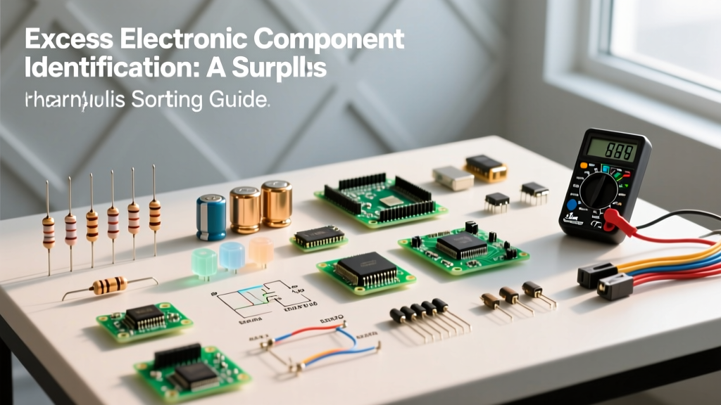

The Hidden Liability of Unsorted Surplus
In 2026, as global supply chains for specialized analog ICs and power semiconductors continue to experience localized bottlenecks, maintaining a robust internal inventory is more critical than ever. However, makers, university labs, and small production houses all share one common problem: bins full of unsorted, unlabeled, or partially used tape-and-reel stock. When you pull an excess electronic component from a disorganized bin, how do you verify it is still viable for a mission-critical PCB prototype?
Managing an excess electronic component inventory requires more than just reading faded silkscreens. It demands a systematic approach to dimensional decoding, electrical verification, and moisture sensitivity management. This guide provides a rigorous, lab-tested protocol for identifying, sorting, and validating surplus components, ensuring your stockpile remains a valuable asset rather than a liability.
Step 1: Visual Inspection and Dimensional Decoding
When dealing with unmarked surface-mount device (SMD) components, your first line of defense is high-magnification visual inspection. Standard 10x jeweler's loupes are insufficient for modern micro-packages. You need a digital microscope with edge-lighting capabilities, such as the Dino-Lite AM73915MT, to inspect pad geometries and pin-1 indicators without glare.
Measuring Pin Pitch and Package Footprints
Many surplus ICs lose their anti-static bags and part numbers, leaving only the physical package. Use digital calipers (accurate to 0.01mm) to measure the pin pitch. Distinguishing between a TSSOP-16 (0.65mm pitch) and a QSOP-16 (0.635mm pitch) by eye is nearly impossible, but a caliper measurement instantly narrows down the footprint family.
- 0402 (1005 Metric) Passives: Measure exactly 1.00mm x 0.50mm. If it measures 0.60mm x 0.30mm, you are holding an 0201 (0603 Metric) component, which requires entirely different stencil apertures.
- SOT-23 vs. SOT-323: Both are 3-pin transistor packages, but the SOT-323 (SC-70) is significantly smaller (2.0mm x 1.25mm) compared to the SOT-23 (2.9mm x 1.3mm).
- QFN vs. DFN: Look for the exposed thermal pad on the bottom. Quad Flat No-lead (QFN) has pads on all four sides, while Dual Flat No-lead (DFN) only has pads on two sides.
Step 2: Decoding Silkscreen, Laser Marks, and Date Codes
Once the package is identified, the next step is decoding the manufacturer's markings. Most active semiconductors feature a 4-digit date code formatted as YYWW (Year and Work Week). For example, a marking of 2345 indicates the part was manufactured in the 45th week of 2023.
Expert Insight: Date codes are not just for inventory rotation; they are critical for solderability. According to solderability standards outlined by IPC, components with matte-tin finishes older than two years are at high risk for oxidation and tin whisker growth, which can cause catastrophic short circuits in high-impedance analog circuits.
Lot Traceability and Manufacturer Logos
Look for subtle laser-etched logos. Texas Instruments often uses a stylized 'TI' or a specific map pin logo, while Analog Devices uses the 'AD' monogram. Cross-reference these markings with the manufacturer's official package drawing documents. If the font weight, alignment, or laser depth looks inconsistent, flag the part for counterfeit screening.
Step 3: Electrical Verification of Passives and Semiconductors
Visual identification only gets you halfway. To truly validate an excess electronic component, you must test its electrical characteristics. Degradation over time affects different component classes in unique ways.
| Component Class | Primary Degradation Risk | Recommended Test Equipment | Pass/Fail Criteria |
|---|---|---|---|
| Electrolytic Capacitors | Electrolyte evaporation, increased ESR | Peak Atlas ESR70 or Siglent LCR meter | ESR within 15% of datasheet spec; Capacitance within -10%/+20% |
| CMOS ICs & Microcontrollers | Input diode degradation, latch-up risk | Semiconductor Curve Tracer (e.g., CurveTracer.com) | Symmetrical IV curves on all I/O pins; no leakage on VCC |
| Power MOSFETs | Gate oxide breakdown, RDS(on) drift | Keysight B1505A or basic multimeter diode test | Gate-to-Source resistance >1MΩ; Body diode drop ~0.4V-0.6V |
| SMD Connectors | Contact oxidation, spring fatigue | Milliohm meter (4-wire Kelvin measurement) | Contact resistance strictly <50mΩ per pin |
For passives like resistors and ceramic capacitors (MLCCs), a high-precision LCR meter is mandatory. MLCCs are prone to micro-cracking if stored improperly or subjected to mechanical shock. A capacitance reading that is significantly lower than the marked value almost always indicates internal dielectric fracturing.
Step 4: Managing Moisture Sensitivity Levels (MSL) in Surplus
Perhaps the most dangerous hidden flaw in surplus SMD components is moisture absorption. Plastic-encapsulated ICs are hygroscopic. If an excess electronic component has been sitting on a shelf outside its moisture barrier bag (MBB) with a compromised humidity indicator card (HIC), water vapor has penetrated the epoxy resin.
The Popcorn Effect
When a moisture-compromised IC passes through a 260°C lead-free reflow oven, the trapped water instantly vaporizes into steam. The resulting internal pressure causes the package to delaminate or crack—a phenomenon known as the 'popcorn effect'. This creates micro-fissures that lead to immediate field failure or long-term corrosion.
Guidelines established by the JEDEC Solid State Technology Association under the J-STD-033 standard dictate strict floor life limits based on the component's MSL rating:
- MSL 1: Unlimited floor life at ≤30°C/85% RH.
- MSL 2: 1 year floor life.
- MSL 3: 168 hours (1 week) floor life. Common for buck converters and motor drivers.
- MSL 4: 72 hours (3 days) floor life.
- MSL 5 & 6: 48 hours and 24 hours, respectively. Common for high-pin-count BGAs and QFNs.
Baking Protocols for Reclamation
If you discover an MSL 3 or higher component with an unknown exposure time, you must bake it before reflow soldering. Standard reclamation baking requires placing the parts in a convection oven at 125°C for 4 to 8 hours (depending on package thickness). Warning: Never bake components in carrier tubes or plastic trays not rated for high temperatures, as they will warp and contaminate the leads. Use high-temperature JEDEC trays or metal baskets.
Step 5: Spotting Counterfeits in Secondary Market Surplus
If your excess inventory was sourced from unauthorized brokers or secondary market liquidators, the risk of counterfeit components is high. Counterfeiters often take obsolete, low-value chips, sand off the original markings (a process called 'blacktopping'), and print fake logos of expensive, high-demand microcontrollers.
The Acetone and Scratch Tests
Genuine manufacturer markings are typically laser-etched into the epoxy or applied with highly resilient, aerospace-grade inks. Counterfeiters often use cheap toner or painted overlays.
- The Acetone Test: Soak a cotton swab in pure acetone and rub the top of the IC firmly for 10 seconds. If the markings smear, fade, or the swab turns black, the part is almost certainly counterfeit.
- The Scratch Test: Gently scrape the surface with a brass pick. Genuine laser marks will feel etched into the substrate. Fake painted marks will flake off, revealing a different colored epoxy or older date codes underneath.
- X-Ray Inspection: For high-value BGA processors, internal die inspection via X-ray is the only definitive test. The NASA Electronic Parts and Packaging (NEPP) Program maintains extensive databases on counterfeit die sizes and internal wire-bonding anomalies to help labs verify silicon authenticity.
Frequently Asked Questions
Can I use an excess electronic component if the leads are oxidized?
It depends on the severity. Light yellowing on matte-tin leads can often be remedied by tinning the leads with a soldering iron and fresh, flux-cored solder (e.g., Kester 245) before automated placement. However, if the oxidation is dark grey or pitted, the component will cause voiding in the solder joints and should be scrapped.
How do I identify an unmarked SMD diode?
Use a multimeter's diode test mode. A standard silicon switching diode (like the 1N4148 equivalent) will show a forward voltage drop of roughly 0.6V to 0.7V. A Schottky diode (like the BAT54) will read between 0.2V and 0.4V. If it reads open in both directions, it is either a blown diode, a capacitor, or an RF tuning diode requiring an LCR meter for identification.
What is the best way to store sorted surplus inventory?
Store moisture-sensitive ICs in resealable ESD-safe Mylar bags with fresh desiccant packs and a 5% humidity indicator card. Keep the storage environment climate-controlled at 25°C and 40% relative humidity. For passives, use compartmentalized ESD-safe bins, but ensure the original tape-and-reel packaging is kept intact to prevent component loss and to preserve the manufacturer's lot codes.