
The Hidden Cost of Disorganized Bins in Circuit Prototyping
Every hardware engineer and DIY maker has experienced the 'missing component' bottleneck. You are halfway through soldering a custom microcontroller board, only to realize you are out of 10kΩ 0603 resistors, or worse, you cannot distinguish your 10kΩ from your 100kΩ resistors in a chaotic storage bin. As we move through 2026, the DIY community has largely standardized on advanced ECAD tools like KiCad 8.x for schematic capture, yet the physical handling of components often remains stuck in the past. An electronic component organizer is not just a storage box; when paired with a systematic 'kitting' workflow, it becomes a critical manufacturing tool that bridges the gap between digital design and physical assembly.
Selecting the Right Electronic Component Organizer Hardware
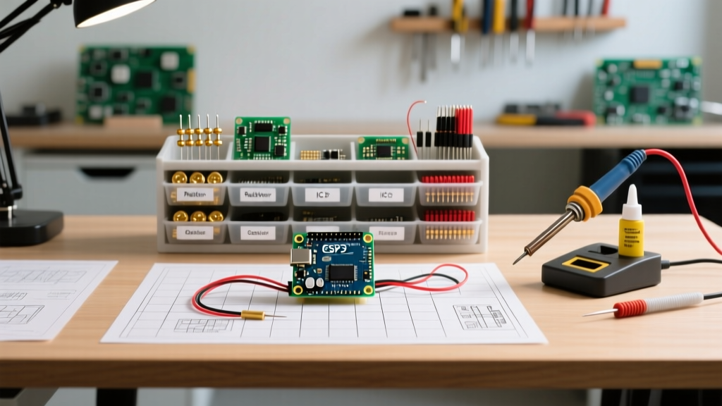
Not all plastic bins are created equal. The wrong choice leads to sagging drawers, static discharge damage, and label degradation. Here is a technical breakdown of the top-tier organizers used in professional prototyping labs, complete with real-world pricing and failure modes.
1. Akro-Mils 10164 (64-Drawer Cabinet)
- Price Range: $32 - $38
- Dimensions: 2-1/8" W x 1-1/2" H x 5-1/2" D per drawer
- Best For: Through-hole components, connectors, and 0805/0603 SMD tape strips.
- Failure Mode: The polystyrene plastic is not inherently ESD-safe. Storing bare, moisture-sensitive ICs directly in these drawers without shielding can lead to electrostatic damage over time.
2. Desco 19250 (ESD-Safe Bin Box)
- Price Range: $85 - $110
- Material: Static-dissipative surface resistance (10^6 to 10^9 ohms/sq).
- Best For: Bare microcontrollers, FPGAs, and sensitive MOSFETs.
- Pro Tip: According to Desco Industries, maintaining a continuous path to ground via an ESD mat is required for these bins to function optimally in dry environments.
3. Stanley Deep Pro 25-Compartment (014725R)
- Price Range: $18 - $22
- Best For: Bulk wire spools, terminal blocks, and mechanical hardware (standoffs, screws).
- Failure Mode: The removable dividers can shift if the box is dropped, mixing M3 and M2.5 brass standoffs—a nightmare to sort out.
The BOM-to-Bin Mapping Strategy
A high-quality electronic component organizer is useless without a rigorous taxonomy. The industry standard for labeling relies on the EIA footprint code + Value + Tolerance + Bin ID format. Using a thermal transfer label maker (like the Brother PT-D210 with 12mm TZe synthetic tapes) prevents the label peeling caused by plasticizer off-gassing from cheap PVC dividers.
Labeling Formula: [Value] [Footprint] [Tolerance/Voltage] [Bin Grid]
Example: 10kΩ 0603 1% [C-14]
Always map your physical drawer grid (A1 to H8) to a digital spreadsheet. When you order from Digi-Key or Mouser, download the CSV receipt and append your internal Bin Grid column. This allows you to use Excel's VLOOKUP function to instantly find where a newly arrived component belongs.
Circuit Application Tutorial: Kitting an ESP32-S3 Dev Board
'Kitting' is a manufacturing process where all components for a specific Bill of Materials (BOM) are picked from the main electronic component organizer and staged in a temporary assembly tray before soldering begins. This eliminates the 'pick-and-place' fatigue of walking back and forth to your storage wall during reflow or hand-soldering.
Step 1: Export and Clean the BOM
Using KiCad's BOM generation tool, export your design to CSV. As noted in the official KiCad documentation, customizing the BOM plugin to group identical footprint/value combinations is essential. A single ESP32-S3 custom board might have 45 unique line items, but 110 total physical components.
Step 2: The Staging Process
- Prepare the ESD Mat: Lay out a 3M 4000 series static-dissipative mat and ground it to your bench.
- Deploy the Kitting Tray: Use a multi-compartment silicone tray or a dedicated anti-static petri dish set.
- Pull Components: Using ESD-safe tweezers (e.g., Hakko CHP 7-SA), pull the exact quantities required from your main electronic component organizer.
- Verify MSL Ratings: Check if any pulled ICs require baking before reflow.
ESP32-S3 Kitting Matrix
Below is a snapshot of a real-world kitting matrix for a custom IoT sensor node. Notice how the organizer location directly correlates to the physical pick path to minimize hand movement.
| Ref Des | Component | Footprint | Qty | Organizer Bin | MSL Rating |
|---|---|---|---|---|---|
| U1 | ESP32-S3-WROOM-1 | Module-SMD | 1 | ESD-Bin-04 | MSL 3 |
| R1-R4 | 10kΩ Pull-up | 0603 | 4 | Grid-C-14 | N/A |
| C1, C5 | 100nF Decoupling | 0402 | 2 | Grid-B-02 | N/A |
| U2 | AP2112K-3.3 LDO | SOT-23-5 | 1 | Grid-F-11 | MSL 1 |
| J1 | USB-C Receptacle | 16-Pin SMD | 1 | Drawer-22 | N/A |
Advanced Environmental & ESD Considerations
When organizing surface-mount devices (SMDs), environmental degradation is a silent killer of prototype yields. Understanding Moisture Sensitivity Levels (MSL) is mandatory for modern circuit application workflows.
Managing MSL 3 Components in Your Organizer
High-density RF modules like the ESP32-S3-WROOM-1 are typically rated as MSL 3. This means they have a maximum floor life of 168 hours (7 days) when exposed to ambient factory conditions (≤30°C/60% RH). If your electronic component organizer is located in a non-climate-controlled garage or basement, humidity will quickly exceed these thresholds.
- The Fix: Never store MSL 3+ components loose in standard plastic drawers. Keep them sealed in their original Moisture Barrier Bags (MBB) with the included silica gel and Humidity Indicator Card (HIC).
- Rebaking: If the HIC shows >10% saturation, the components must be baked in a dedicated convection oven at 40°C for 24-48 hours before reflow soldering to prevent the 'popcorn effect' (internal steam explosion cracking the IC package).
- ESD Shielding: For bare ICs, consult the Digi-Key ESD Basics guide to understand why standard pink poly bags are only anti-static, not ESD-shielding. You must use metalized Mylar shielding bags inside your organizer drawers for unshielded microcontrollers.
Pro-Troubleshooting: Common Binning Mistakes
Even with a premium electronic component organizer, workflow errors can halt a build. Avoid these three critical mistakes:
- Mixing Tolerances: Never put 1% and 5% tolerance resistors of the same value in the same bin. When designing precision analog front-ends (like op-amp feedback loops), accidentally grabbing a 5% part will ruin your noise floor and gain accuracy.
- Ignoring Voltage Ratings on Capacitors: A 100nF 0603 capacitor could be rated for 16V or 100V. Physically, they look identical. Always include the voltage rating on your drawer label (e.g., 100nF 0603 X7R 50V) to prevent catastrophic dielectric breakdown on higher-voltage rails.
- Overstuffing Drawers: Forcing SMD tape reels into a drawer that is 1/8" too short causes the tape to crease. When you later try to feed this tape into an automatic pick-and-place machine or even just peel it back with tweezers, the creased cover tape will snap, launching 0402 capacitors across the room.
Conclusion
Treating your electronic component organizer as an active participant in your circuit application tutorial—rather than a passive closet—drastically reduces prototyping friction. By implementing BOM-to-bin mapping, enforcing strict MSL storage protocols, and utilizing a dedicated kitting workflow, you transform your workbench from a chaotic hobby space into a streamlined, professional-grade hardware lab.