
The Core Question: What Is an NPN Transistor?
If you are diving into PCB prototyping or repairing analog circuitry, you have inevitably asked: what is npn transistor technology, and how does it actually work? At its most fundamental level, an NPN (Negative-Positive-Negative) transistor is a three-terminal semiconductor device used to amplify or switch electronic signals. It consists of three layers of doped silicon: an N-type emitter, a P-type base, and an N-type collector.
Unlike PNP transistors, which rely on the movement of 'holes' (positive charge carriers), NPN transistors utilize electrons as their majority carriers. Because electrons move through silicon roughly two to three times faster than holes, NPN transistors inherently offer better high-frequency performance and lower noise. This makes them the undisputed workhorse of modern discrete electronics.
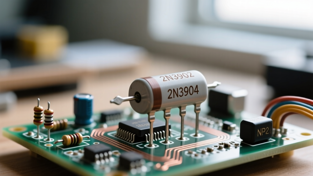
To truly understand how to use them, we must move beyond textbook definitions and look at real silicon. In this guide, we will perform a complete datasheet breakdown of the legendary 2N3904, the most ubiquitous general-purpose NPN BJT (Bipolar Junction Transistor) in the DIY and commercial prototyping space.
Decoding the 2N3904 Datasheet: Pinout and Package
The 2N3904 is typically housed in a TO-92 through-hole package or an SOT-23 surface-mount package. For breadboard prototyping, the TO-92 is standard. A common pitfall for beginners is misidentifying the pinout, which leads to immediate component failure upon powering the circuit.
Standard TO-92 Pin Identification
When holding the transistor with the flat edge facing you and the leads pointing downward, the pins from left to right are:
- Emitter (E): The source of electrons. Usually tied to ground in common-emitter configurations.
- Base (B): The control terminal. A small current here dictates a massive current flow from Collector to Emitter.
- Collector (C): The terminal that collects the electrons. Connected to the load or positive supply.
Always verify the pinout against the specific manufacturer's datasheet. While E-B-C is standard for the 2N3904, other NPN transistors like the BC547 use a completely different C-B-E arrangement.
Absolute Maximum Ratings: Where the Magic Dies
The 'Absolute Maximum Ratings' table is not a target; it is a cliff edge. Exceeding these values will cause permanent silicon degradation or catastrophic thermal failure. According to the ON Semiconductor 2N3904 Product Page, the hard limits at 25°C are:
- Collector-Emitter Voltage (VCEO): 40V
- Collector Current (IC): 200mA (Continuous)
- Total Device Dissipation (PD): 625mW
The Hidden Danger: Thermal Derating
Many hobbyists miss the derating curve. The 625mW power limit is only valid at an ambient temperature of 25°C. The datasheet specifies a derating factor of 5.0 mW/°C. If your enclosure heats up to 85°C, you must subtract (60°C × 5mW) = 300mW from your maximum limit. Your new safe power dissipation is just 325mW. Designing a circuit that pushes 150mA at 12V (1.8W) through a 2N3904 will result in a tiny, smoky pop.
DC Current Gain (hFE): The Heart of Amplification
The DC Current Gain, denoted as hFE or Beta (β), defines the ratio of Collector current to Base current (IC / IB). It is the metric that tells you how much 'amplification' you get. However, hFE is notoriously unstable. It varies wildly with temperature, collector current, and manufacturing batches.
Below is a breakdown of the 2N3904 hFE bins as specified at VCE = 1.0V:
| Collector Current (IC) | Minimum hFE | Maximum hFE | Practical Takeaway |
|---|---|---|---|
| 1.0 mA | 40 | - | Low-current amplification is weak; avoid using for high-gain preamps. |
| 10 mA | 80 | 300 | The 'sweet spot' for linear analog amplification. |
| 100 mA | 30 | - | Gain drops heavily at high currents (Kirk Effect). Do not rely on high beta here. |
For a deeper dive into the semiconductor physics governing these variations, the All About Circuits BJT Introduction provides excellent foundational theory on minority carrier injection.
Switching vs. Linear: VCE(sat) and Base Drive
When prototyping digital logic or driving relays with microcontrollers, we do not use the transistor as a linear amplifier; we use it as a switch. In this mode, we want the transistor to be fully 'ON', meaning the voltage drop across the Collector and Emitter (VCE) should be as close to zero as possible.
This is known as the Collector-Emitter Saturation Voltage (VCE(sat)). For the 2N3904:
- At IC = 10mA and IB = 1mA, VCE(sat) is typically 0.2V.
- At IC = 50mA and IB = 5mA, VCE(sat) rises to 0.3V.
Notice the ratio of IC to IB in these tests is exactly 10. This is a crucial concept called Forced Beta. To guarantee an NPN transistor enters hard saturation, you must artificially force the Beta to 10, regardless of what the hFE table says. If your load requires 100mA, you must supply at least 10mA to the Base.
Real-World Prototyping: Sizing the Base Resistor
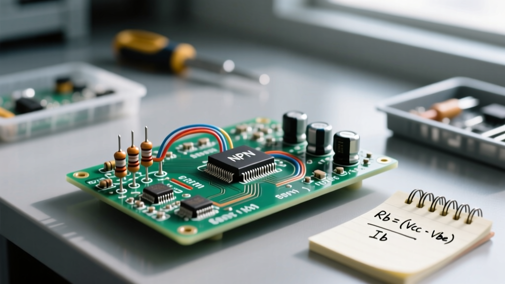
Let us apply this datasheet knowledge to a common scenario: switching a 12V, 50mA relay coil using a 5V Arduino GPIO pin. As outlined in community troubleshooting threads like this SparkFun Transistors Tutorial, calculating the base resistor is mandatory to protect both the microcontroller and the BJT.
Step-by-Step Calculation
- Identify Required Collector Current (IC): 50mA (Relay coil).
- Determine Base Current (IB) using Forced Beta (10): IB = 50mA / 10 = 5mA.
- Calculate Voltage across Base Resistor: Arduino outputs 5V. The Base-Emitter junction drops roughly 0.7V. V_R = 5V - 0.7V = 4.3V.
- Apply Ohm's Law: R = V_R / IB = 4.3V / 0.005A = 860 Ohms.
Select the next lowest standard E12 resistor value to guarantee enough base drive: 820 Ohms. Using a 1k or 10k resistor here is a common hobbyist mistake that leaves the transistor in the 'active' (linear) region, causing it to overheat and fail while driving inductive loads.
Common Failure Modes in Prototyping
Even with perfect math, NPN transistors face specific real-world hazards on the prototyping bench:
- Inductive Kickback: If you are switching a relay or motor without a flyback diode, the collapsing magnetic field generates a massive reverse voltage spike. This exceeds the 40V VCEO limit, resulting in avalanche breakdown and a shorted Collector-Emitter junction.
- Secondary Breakdown: If the transistor is subjected to high voltage and high current simultaneously (common in linear power supplies), localized hotspots form on the silicon die, melting the internal junctions in microseconds.
- Base-Emitter Reverse Breakdown: The B-E junction acts like a weak Zener diode (typically around 6V). If an AC signal or negative voltage spike hits the base, it will punch through the junction, permanently dropping the transistor's hFE.
Summary for the Workbench
Understanding what is npn transistor technology goes far beyond the simple 'water valve' analogy. By reading the absolute maximum ratings, respecting the thermal derating curves, and designing for forced Beta saturation rather than relying on arbitrary hFE values, you transition from guessing to engineering. The 2N3904 remains an exceptional, low-cost (~$0.03 per unit in bulk) component for switching loads up to 100mA and building discrete logic gates, provided you treat its datasheet as the ultimate rulebook.