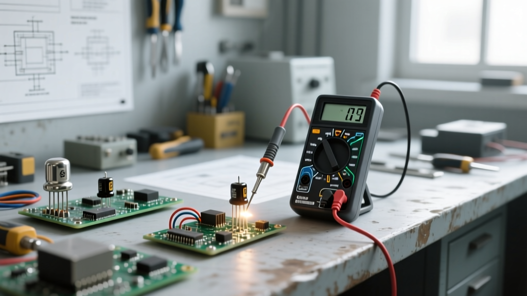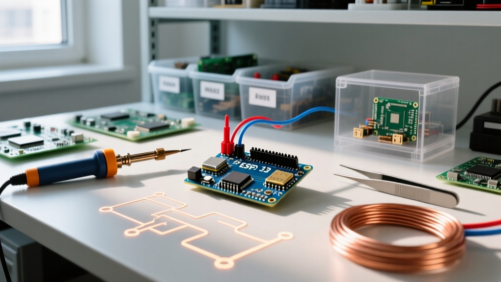

The modern electronics ecosystem operates on a razor-thin margin of redundancy. While consumer attention often fixates on cutting-edge 3nm processors for smartphones and AI servers, the backbone of industrial control, IoT prototyping, and automotive systems relies on legacy silicon and passive components. As we navigate 2026, the electronic component supply shortage continues to disrupt hardware development, not because of a lack of raw silicon, but due to deeply entrenched structural bottlenecks in fabrication, packaging, and distribution allocation. Understanding the mechanical and economic realities of this gridlock is essential for electrical engineers and DIY makers who need to transition from breadboard concepts to manufactured PCBs without stalling their projects.
The Anatomy of a Silicon Bottleneck: Front-End Fabrication
To understand why a simple 8-bit microcontroller or an analog op-amp remains difficult to source, we must look at the front-end fabrication process. The semiconductor industry has aggressively transitioned to 300mm (12-inch) wafer production for advanced logic and memory. However, the vast majority of power management ICs (PMICs), display drivers, and legacy microcontrollers (like the ubiquitous STM32F103 series) are manufactured on older 200mm (8-inch) wafer lines.
Building a new 200mm fabrication plant (fab) is economically unviable in 2026. The capital expenditure required cannot be justified by the low profit margins of legacy chips, which often sell for under $1.50 in high volumes. Consequently, global 200mm fab capacity is essentially capped. According to data tracked by the Semiconductor Industry Association (SIA), utilization rates for legacy nodes consistently hover above 90%, leaving zero buffer for demand spikes. When a maker or small-batch assembler requires 5,000 units of a specific analog-to-digital converter, they are competing for the fractional percentage of wafer starts that Tier 1 automotive and medical OEMs have not already locked up via multi-year agreements.
The Back-End Gridlock: OSAT and Substrate Chemistry
Even when wafers are successfully fabricated, they must undergo assembly and testing at Outsourced Semiconductor Assembly and Test (OSAT) facilities. This back-end process has become a severe choke point, driven largely by advanced packaging requirements and substrate material shortages.
The MLCC Sintering Constraint
Passive components, specifically Multi-Layer Ceramic Capacitors (MLCCs), suffer from a completely different set of physical constraints. High-capacitance MLCCs, such as the Murata GRM series, require barium titanate dielectric layers stacked hundreds of times at microscopic thicknesses. The critical bottleneck here is the sintering process. These ceramic stacks must be baked in specialized kilns at temperatures exceeding 1,200°C for extended periods to achieve the correct crystalline structure. You cannot simply 'spin up' a new MLCC kiln in a matter of months; the capital cost and calibration time span years. When demand for consumer electronics or EVs surges, kiln capacity maxes out, leading to 30-to-40-week lead times for specific 0402 and 0603 footprint capacitors.
ABF Substrate Limitations
For complex microcontrollers and FPGAs utilizing Ball Grid Array (BGA) or Quad Flat No-lead (QFN) packages, the substrate is critical. Ajinomoto Build-up Film (ABF) remains the industry standard for high-performance substrates. The chemical synthesis and curing processes for ABF are highly specialized, and capacity expansions by chemical suppliers have historically lagged behind the exponential growth in pin-counts required by modern MCUs. This means perfectly good silicon dice can sit in storage for months waiting for the physical packaging materials required to mount them to a PCB.
2026 Market Reality: Lead Times and Pricing by Component Class
The impact of these mechanical bottlenecks is starkly visible in the distribution market. Below is a snapshot of average lead times and spot-market pricing shifts for commonly used prototyping and low-volume production components as of early 2026.
| Component Class | Example Part Number | Pre-2021 Lead Time | 2026 Spot Lead Time | Price Shift (1k Reel) |
|---|---|---|---|---|
| 32-bit ARM MCU | STM32F103C8T6 | 10-12 Weeks | 45-52 Weeks | $2.10 to $11.50 |
| General Purpose Op-Amp | LM358P (SOIC-8) | 6-8 Weeks | 22-26 Weeks | $0.18 to $0.85 |
| MLCC (0603, 100nF) | Murata GRM188R71H104KA93D | 8-10 Weeks | 14-18 Weeks | $0.004 to $0.025 |
| Switching Voltage Regulator | TPS5430DDAR (TI) | 12 Weeks | 35-40 Weeks | $1.80 to $5.20 |
As highlighted by recent supply chain resilience reports from the NIST CHIPS program, the strategic stockpiling of legacy analog and power components has become a matter of national security, further squeezing the commercial and hobbyist markets as government-subsidized manufacturers absorb available inventory.
The Allocation Hierarchy: Where Prototypers Fit In
Franchise distributors like Arrow, Avnet, and Mouser operate on an allocation hierarchy. When a component enters a shortage phase, available stock is not distributed on a first-come, first-served basis. Instead, algorithms prioritize allocations based on customer tier, historical volume, and end-market criticality (e.g., life-saving medical devices and automotive safety systems take precedence).
For the DIY engineer, university research lab, or small-batch design house ordering via Digi-Key or Mouser in quantities under 10,000, this means hitting a 'wall' on product pages. You are effectively placed at the back of the queue. To bypass this, hardware developers must shift their strategy from sourcing to designing for availability.
Tactical PCB Design Strategies to Bypass Allocation Queues
Surviving the electronic component supply shortage in 2026 requires embedding supply-chain awareness directly into your EDA (Electronic Design Automation) workflow. Here are three actionable engineering strategies to insulate your prototypes from allocation gridlock.
1. Adaptive Footprint Engineering
Never design a PCB footprint that accepts only a single manufacturer's package. By utilizing adaptive pad geometries, you can create a single footprint that accommodates multiple package variations. For example, an extended SOIC-8 pad layout can be designed to also accept an MSOP-8 or TSSOP-8 part by elongating the copper pads inward and outward. This allows your assembly house (like PCBWay or JLCPCB) to source whichever op-amp or voltage reference is currently in stock from any vendor (TI, ST, Microchip, or Diodes Inc.) without requiring a board respin.
2. Strategic Passive Derating
Commodity passives often face localized shortages based on voltage ratings. A standard 16V, 100nF 0603 MLCC might have a 30-week lead time due to massive demand in consumer IoT devices. However, a 50V or 100V equivalent from the same manufacturer might be sitting in stock with a 4-week lead time. The price penalty for over-specifying the voltage rating on a low-voltage (3.3V or 5V) rail is often just fractions of a cent per unit, but it grants you access to a completely different, less-contested inventory pool. Always check distributor API stock levels for higher-voltage variants before finalizing your BOM.
3. Multi-Source BOM Architectures
Design your schematic with 'alternate' part numbers natively integrated into the component properties. Modern EDA tools like Altium Designer and KiCad allow you to define secondary and tertiary manufacturer part numbers (MPNs) for every symbol. When you export your BOM and CPL (Component Placement List) files, include these alternates. According to market analyses by IPC (Association Connecting Electronics Industries), design houses that implement automated BOM scrubbing and multi-source validation reduce their prototyping delays by up to 60% compared to those relying on single-source legacy components.
Engineering Maxim for 2026: A circuit is only as robust as its weakest supply chain link. Designing a brilliant power topology using a highly specialized, single-source PMIC is a critical failure mode if that IC is trapped in a 52-week OSAT packaging queue. Standardize on boring, multi-sourced silicon whenever possible.
Conclusion
The electronic component supply shortage is no longer a temporary anomaly caused by pandemic-era demand spikes; it is the new structural reality of the global semiconductor industry. The physical limitations of 200mm wafer fabs, the chemical bottlenecks of MLCC sintering, and the rigid allocation hierarchies of franchise distributors dictate the pace of hardware innovation. By understanding the mechanical 'how' and 'why' behind these shortages, electrical engineers and makers can adapt. Through adaptive footprint design, strategic voltage derating, and aggressive multi-source BOM planning, you can ensure your prototypes make it from the breadboard to the final PCB assembly without becoming collateral damage in the global silicon gridlock.