
The Metallurgy of Solder Tinning: Why Base Metals Matter
Solder tinning is the critical preparatory step of coating a base metal, component lead, or wire with a thin, uniform layer of solder alloy. This process serves two primary functions: it prevents surface oxidation prior to the final soldering operation and dramatically improves wetting when the final joint is made. However, the success of solder tinning is entirely dependent on material compatibility. A solder alloy and flux combination that perfectly tins bare copper will fail catastrophically on aluminum or stainless steel.
At a metallurgical level, tinning requires the formation of an Intermetallic Compound (IMC) layer between the tin (Sn) in the solder and the base metal. The thermodynamics of this reaction dictate the required thermal profile, the necessary flux chemistry to remove surface oxides, and the specific alloy composition to ensure long-term reliability. According to the NASA-STD-8739.3 workmanship standards, proper tinning must result in a continuous, smooth, and bright coating without evidence of dewetting or non-wetting. Achieving this across diverse substrates requires a deep understanding of material-specific behaviors.
Material Compatibility Matrix: Base Metals vs. Solder Alloys
Selecting the correct alloy and flux is the first step in any tinning operation. The table below outlines the baseline compatibility for common electrical and mechanical substrates.
| Base Metal | Recommended Solder Alloy | Flux Classification | Tinning Difficulty | Primary Failure Mode |
|---|---|---|---|---|
| Bare Copper | Sn63Pb37 / SAC305 | ROM0 / ROM1 (Rosin) | Low | Excessive IMC growth |
| Brass / Bronze | Sn60Pb40 / Sn96.5Ag3.0Cu0.5 | ROM1 / Water-Soluble | Low-Medium | Zinc leaching / Dewetting |
| Nickel / ENIG | SAC305 / Sn96.5Ag3.5 | Low-Solids No-Clean | Medium | Gold embrittlement |
| Stainless Steel | Sn50Pb50 / Sn99.3Cu0.7 | High-Acid (Zinc Chloride) | High | Non-wetting / Corrosion |
| Aluminum | In51Sn49 / Sn-Zn Alloys | Specialized Halide / Ultrasonic | Extremely High | Oxide barrier rejection |
Deep Dive: Tinning Problematic Surfaces
While copper and tin-lead alloys are inherently compatible, modern electronics and specialized electromechanical assemblies frequently require tinning far more challenging materials.
Aluminum and the Oxide Barrier
Tinning aluminum is notoriously difficult due to the instantaneous formation of aluminum oxide (Al2O3) when the bare metal is exposed to air. This oxide layer is only nanometers thick but is incredibly dense and possesses a melting point of over 2,000°C—far exceeding the melting point of the aluminum substrate itself (660°C) and any standard solder alloy. Standard rosin or no-clean fluxes cannot chemically breach this barrier.
To successfully tin aluminum, manufacturers typically rely on one of two methods:
- Ultrasonic Tinning: Using an ultrasonic soldering iron, high-frequency acoustic cavitation physically shatters the oxide layer in the liquid solder pool, allowing the molten alloy (often a Tin-Zinc or Indium-Tin blend) to wet the bare aluminum before the oxide can reform.
- Aggressive Halide Fluxes: Specialized fluxes containing heavy halides can chemically etch the oxide, but they leave behind highly corrosive residues that mandate rigorous aqueous cleaning. Furthermore, Indium Corporation notes that Indium-based solders (like In51Sn49) exhibit a uniquely high metallurgical affinity for aluminum, making them the premier choice for cryogenic and aerospace aluminum tinning.
Stainless Steel and Nickel Plating
Stainless steel owes its corrosion resistance to a passive chromium oxide layer. This same layer prevents solder wetting. Tinning stainless steel requires highly activated acid fluxes (such as zinc chloride or hydrochloric acid-based formulations). While these fluxes successfully strip the chromium oxide, they introduce a severe risk of galvanic corrosion and ionic contamination if not perfectly cleaned post-tinning.
Nickel, often used as a barrier layer in PCB surface finishes like ENIG (Electroless Nickel Immersion Gold), presents a different challenge. During the tinning of an ENIG pad, the thin gold layer rapidly dissolves into the molten tin. The actual metallurgical bond forms between the tin and the underlying nickel, creating a Ni3Sn4 IMC layer. If the tinning temperature is too low, the gold fails to fully dissolve, leading to weak, brittle joints prone to mechanical fracture.
Flux Chemistry: The Unsung Hero of Wetting
Material compatibility is not just about the metal and the solder; it is equally about the flux. The IPC J-STD-004 standard classifies fluxes based on their chemical composition and activity levels. Choosing the wrong flux for a specific base metal will result in immediate tinning failure.
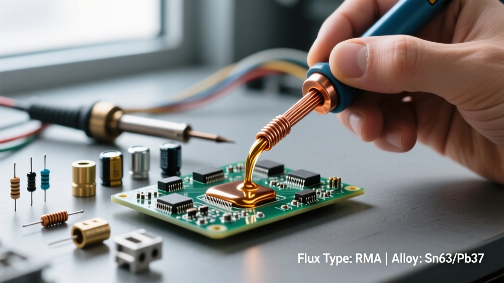
- RO (Rosin-Based): Derived from pine sap, rosin fluxes are mildly active when heated and inert when cool. They are ideal for tinning easily oxidized metals like copper and silver. According to the Kester Flux Chemistry Guide, RMA (Rosin Mildly Activated) remains the gold standard for tinning high-reliability aerospace wiring.
- OR (Organic Acid / Water-Soluble): These fluxes contain stronger organic acids (like lactic or stearic acid) and are necessary for tinning heavily oxidized copper or brass. They must be cleaned with deionized water post-tinning to prevent electrochemical migration.
- IN (Inorganic Acid): Containing strong mineral acids or halide salts, these are strictly reserved for tinning difficult metals like stainless steel, Kovar, or nickel alloys. They are never used in standard PCB electronics manufacturing due to extreme corrosivity.
Troubleshooting Common Tinning Failures
Even with the correct alloy and flux, thermal mismanagement can ruin the tinning process. Understanding the visual and physical difference between non-wetting and dewetting is crucial for root-cause analysis.
Non-Wetting vs. Dewetting
Non-wetting occurs when the molten solder refuses to spread across the base metal, forming discrete beads with a contact angle greater than 90 degrees. This indicates that the flux failed to remove the surface oxide, or the base metal temperature did not reach the liquidus point of the solder alloy. The surface energy of the base metal remains lower than the surface tension of the liquid solder.
Dewetting is a more insidious failure. The solder initially wets the surface, but as heating continues, it retracts into isolated islands, exposing the underlying IMC layer.
Expert Insight: Dewetting is frequently misdiagnosed as a flux contamination issue. In reality, it is most often a thermal management failure. Prolonged exposure to excessive heat drives rapid, excessive growth of the Cu6Sn5 intermetallic layer on copper substrates. The remaining liquid solder rejects this brittle, high-melting-point IMC surface, causing the solder to pull back and dewet.
Preventing Gold Embrittlement in ENIG Tinning
When tinning wires or components to ENIG surfaces, using a solder alloy with a high tin content and insufficient thermal mass can lead to gold embrittlement. If the gold (Au) concentration in the solder joint exceeds 3% by weight, the joint becomes mechanically brittle. To prevent this during the tinning phase, technicians must ensure the solder pot or iron is hot enough (typically 350°C for SAC305) to allow the gold to fully diffuse into the bulk solder matrix, and the tinned wire should be dipped in a fresh solder bath to 'wash' away the gold-heavy solder before making the final connection.
Sourcing and Quality Standards for Tinning Wire
For high-reliability applications, pre-tinned wire (often referred to as tinned copper wire) is purchased rather than tinned in-house. When sourcing tinned wire, verify that the manufacturer adheres to ASTM B331 or IPC-A-620 standards. The tin coating must be a minimum of 40 microinches (1 micron) thick to ensure adequate shelf life and prevent the underlying copper from oxidizing through the tin layer. Always request a certificate of conformance (CoC) detailing the specific alloy used for the tinning process, as substituting a matte tin finish with a bright tin finish (which contains organic brighteners) can introduce outgassing and voiding issues during subsequent wave or reflow soldering operations.