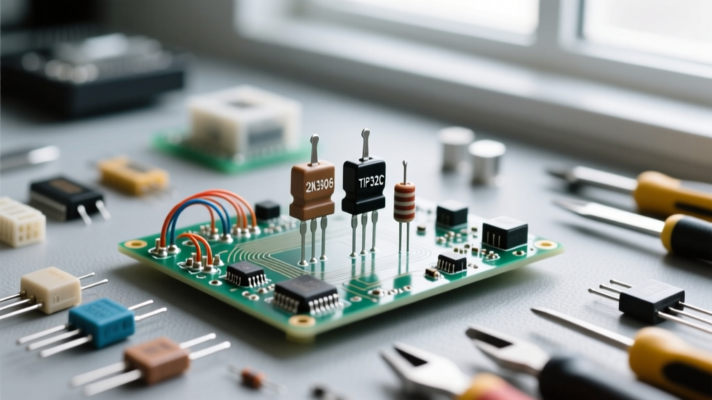

The Architectural Role of PNP Transistors in Modern Prototyping
While NPN bipolar junction transistors (BJTs) often dominate beginner tutorials due to their intuitive low-side switching capabilities, PNP transistors remain indispensable in professional and advanced DIY circuit design. Whether you are designing a precision analog sensor front-end, a high-efficiency switching regulator, or a high-fidelity audio amplifier, the PNP BJT offers unique advantages that NPN devices and MOSFETs simply cannot replicate in certain topologies. In this comprehensive 2026 buying and selection guide, we will dissect the critical parameters, real-world circuit frameworks, and procurement strategies required to master PNP transistor integration.
Unlike NPN transistors, which sink current to ground, PNP transistors source current from the positive supply rail. This fundamental difference dictates their use cases: PNP devices excel at high-side switching, maintaining a common ground reference for the load, and serving as the upper half of complementary push-pull output stages.
Decoding the Datasheet: Critical PNP Specifications
When browsing distributor catalogs, the sheer volume of PNP part numbers can be overwhelming. To narrow down your selection, you must evaluate four primary datasheet parameters. Note that manufacturers often specify PNP voltages and currents as negative values to reflect conventional current flow out of the emitter, though absolute maximum ratings are sometimes listed as positive magnitudes.
Collector-Emitter Breakdown Voltage (VCEO)
This is the maximum voltage the transistor can block between the collector and emitter when the base is open. For a 12V automotive circuit, a PNP with a VCEO of -45V (like the BC557) provides a safe margin. For 24V industrial systems, look for devices rated above -60V, such as the 2N5401.
Continuous Collector Current (IC) and Power Dissipation (PD)
IC defines the maximum continuous current the device can handle. However, current alone is misleading without considering PD. A TO-92 packaged 2N3906 is rated for -200mA, but its PD is only 625mW at 25°C. If you attempt to switch a 12V, 200mA relay coil directly without a flyback diode or if the transistor lingers in the linear region, it will dissipate over 2W during the transition phase, instantly destroying the silicon die.
DC Current Gain (hFE or Beta)
hFE represents the amplification factor. Small-signal PNPs like the BC557C offer gains up to 800, making them ideal for high-impedance sensor interfaces. Power PNPs like the TIP32C have much lower gains (typically 10 to 50), requiring robust base drive circuits.
2026 Component Shortlist: Signal, Power, and Darlington PNPs
To streamline your prototyping workflow, stock your lab with these proven, widely available PNP workhorses. The following comparison chart highlights the best options across different power domains.
| Model | Category | VCEO | IC (Max) | hFE Range | Package | Primary Application |
|---|---|---|---|---|---|---|
| BC557 | Small Signal | -45V | -100mA | 125 - 800 | TO-92 | Audio preamps, logic level shifting |
| 2N3906 | Small Signal | -40V | -200mA | 100 - 300 | TO-92 | General switching, LED drivers |
| 2N5401 | High Voltage | -150V | -500mA | 60 - 300 | TO-92 | Telecom, high-voltage regulators |
| TIP32C | Power BJT | -100V | -3A | 10 - 50 | TO-220 | Motor control, linear power supplies |
| TIP127 | Darlington | -100V | -5A | >1000 | TO-220 | High-current loads, MCU interfacing |
Packaging Realities: TO-92 vs. SOT-23 vs. TO-220
The physical package of your PNP transistor dictates not only your assembly method but also its thermal performance. The classic TO-92 through-hole package is excellent for breadboarding and hand-soldering, but its thermal resistance to ambient air (RθJA) is notoriously high, often exceeding 200°C/W. This means a mere 300mW of dissipated power will push the junction temperature 60°C above ambient.
For high-density PCB designs, the SOT-23 surface-mount equivalent (such as the MMBT3906) offers a smaller footprint and slightly better thermal coupling to the PCB copper. However, for power applications exceeding 1W, you must transition to a TO-220 package (like the TIP32C). The TO-220 features an exposed metal tab that can be screwed to a heatsink, dropping the thermal resistance to as low as 2°C/W when properly mated with thermal compound. Always calculate your worst-case power dissipation before locking in your package choice.
Design Framework: High-Side Switching with Microcontrollers
A common trap for DIYers is attempting to drive a high-side PNP transistor directly from a 3.3V or 5V microcontroller GPIO pin. If the PNP emitter is tied to a 12V supply, the base-emitter junction will be forward-biased by 12V when the MCU pin outputs 0V (LOW). This will instantly fry the base junction and likely back-feed and destroy your microcontroller.
The Solution: Use an NPN transistor (like a 2N3904) or an N-channel logic-level MOSFET as a low-side inverter. The MCU drives the NPN base via a current-limiting resistor. When the MCU goes HIGH, the NPN turns on, pulling the PNP base to ground through a resistor, thereby turning the PNP ON and energizing the 12V load. This level-shifting topology is mandatory for safe high-side PNP actuation.
Thermal Runaway and the Necessity of Emitter Degeneration
Bipolar transistors suffer from a negative temperature coefficient regarding their base-emitter voltage (VBE). As the silicon die heats up, the VBE required to maintain a specific collector current drops by approximately 2mV per degree Celsius.
Expert Insight: If you bias a PNP transistor using a fixed voltage divider on the base without an emitter resistor, a 10°C rise in junction temperature will effectively increase the forward bias by 20mV. Because the BJT current-voltage relationship is exponential, this tiny voltage shift can cause the collector current to double, generating more heat, dropping VBE further, and culminating in catastrophic thermal runaway.
To prevent this, always incorporate an emitter degeneration resistor (RE). As collector current rises, the voltage drop across RE increases, which subtracts from the base-emitter bias voltage, inherently stabilizing the operating point through negative feedback.
Complementary Pairs and the Sziklai Topology
In Class AB and Class B audio output stages, PNP and NPN transistors are used in tandem to create a push-pull configuration. For optimal performance and minimal crossover distortion, the PNP and NPN devices must be complementary pairs—meaning they share nearly identical gain curves, transition frequencies (fT), and output capacitances. Classic pairs include the 2N3904/2N3906 for low-power headphone amplifiers, and the TIP31/TIP32 for medium-power speaker drivers.
Another advanced topology utilizing PNP transistors is the Sziklai pair (or complementary feedback pair). Unlike a standard Darlington pair, which uses two transistors of the same polarity, a Sziklai pair combines a PNP driver with an NPN output transistor (or vice versa). This configuration provides the massive current gain of a Darlington but suffers from only a single VBE voltage drop (approx 0.6V) instead of two (1.2V). This makes the Sziklai pair vastly superior for high-side power switching where minimizing voltage drop and heat generation is paramount.
Procurement: Navigating the Counterfeit Component Market
As of 2026, the secondary market remains flooded with counterfeit BJTs. Remarked TO-92 devices are notoriously common; a batch labeled as 2N3906 might actually contain low-gain NPNs or even small-signal diodes that will short your power supply upon installation.
Buying Best Practices:
- Stick to Authorized Distributors: Source components from Mouser, Digi-Key, Farnell, or Newark. The slight premium guarantees authenticity and traceability to the original manufacturer.
- Inspect the Markings: Genuine TO-92 transistors from ON Semiconductor or Diodes Inc. typically use precise, laser-etched or high-quality ink markings. Fakes often feature sloppy, thick font that rubs off with isopropyl alcohol.
- Verify with a Curve Tracer: If you must buy in bulk from unverified sources, use a component tester or curve tracer to verify the hFE and polarity of a random sample before soldering them into a complex PCB.
Final Thoughts on PNP Selection
Selecting the right PNP transistor requires balancing voltage headroom, current demands, and thermal realities. By understanding the nuances of high-side driving, respecting the physics of thermal runaway, and sourcing from reputable suppliers, you can leverage PNP BJTs to build robust, professional-grade electronic systems. For deeper mathematical modeling of BJT biasing networks, refer to the Texas Instruments Analog Engineer's Pocket Reference or consult specific device datasheets like the ON Semiconductor 2N3906 Datasheet. You can also check real-time inventory and pricing for these components on the Mouser Electronics PNP Bipolar Transistors Category.