
The Cognitive Load Bottleneck in Electronics Labs
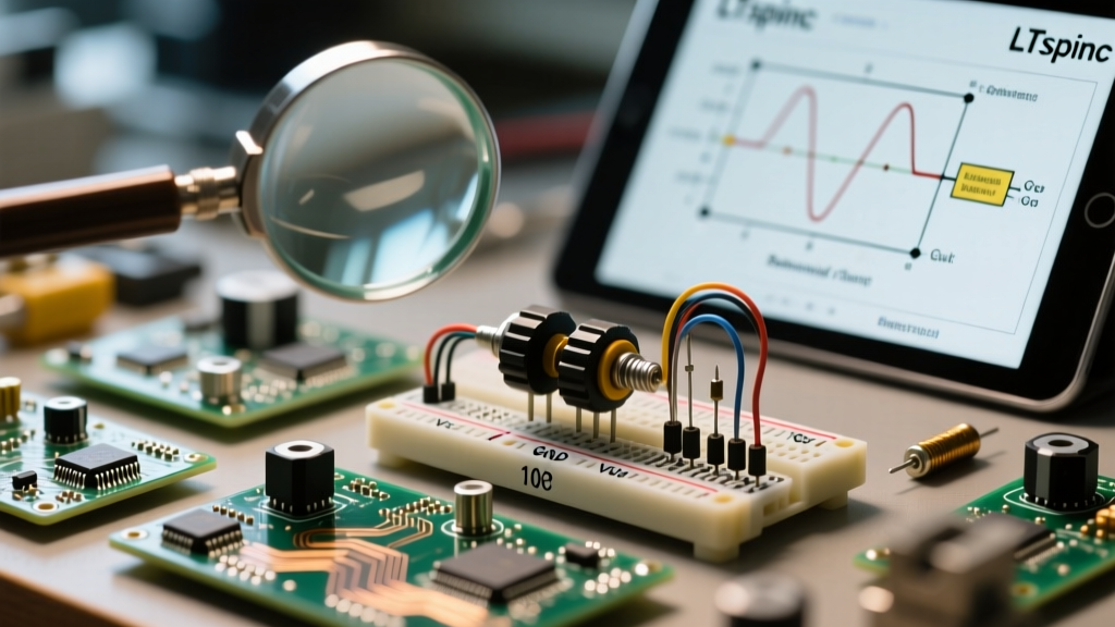
In university engineering labs, maker spaces, and vocational training centers, the 'bin dive' is a notorious momentum killer. When students are tasked with designing and assembling a custom printed circuit board (PCB) or breadboard prototype, they often spend up to 40% of their lab time hunting through disorganized component drawers for a specific 470-ohm resistor or a 100nF decoupling capacitor. From an educational standpoint, this is highly inefficient.
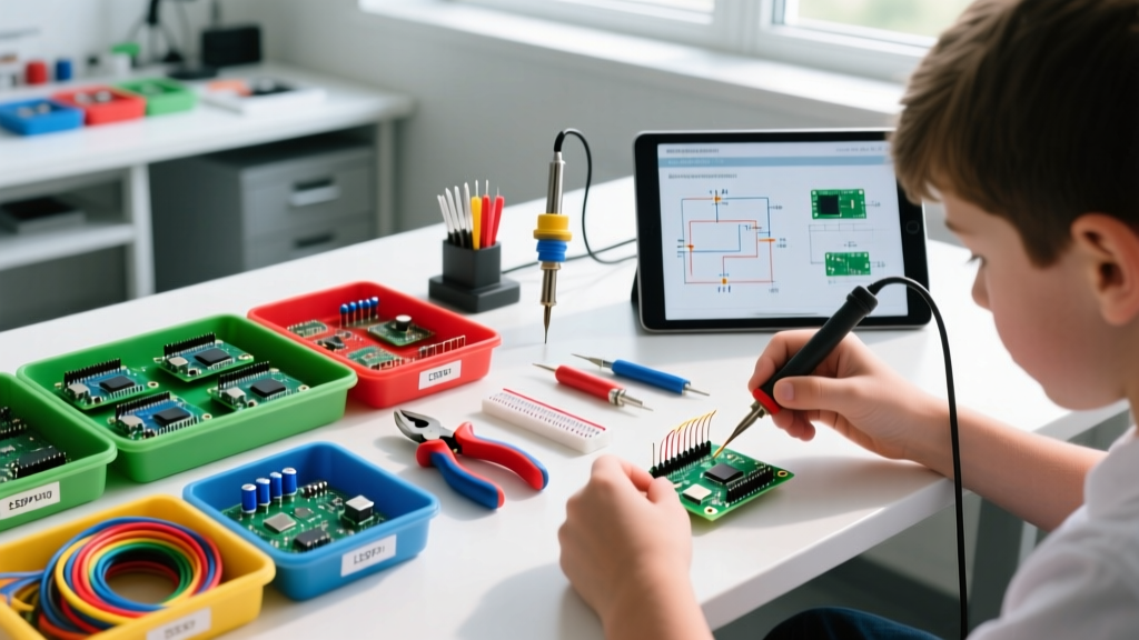
According to research published by the American Society for Engineering Education (ASEE), project-based learning (PBL) thrives when students can maintain a state of flow, focusing on higher-order problem-solving rather than logistical friction. When learners are forced to navigate chaotic shared component bins, their working memory is consumed by visual search tasks—a phenomenon explained by Sweller’s Cognitive Load Theory. By implementing structured electronic component kitting, educators and lab managers can eliminate this friction, transforming the lab experience from a frustrating scavenger hunt into a streamlined engineering workflow.
Defining Electronic Component Kitting for PBL
In a manufacturing context, kitting refers to the process of grouping all necessary parts for a specific assembly into a single package before it reaches the production line. In a Project-Based Learning environment, electronic component kitting serves the exact same purpose but is scaled for educational cohorts. It involves generating a precise Bill of Materials (BOM), procuring exact quantities, verifying component values, and packaging them into individual, ESD-safe student kits prior to the lab session.
The PBL Kitting Principle: A student's cognitive resources should be spent calculating the cutoff frequency of an active low-pass filter, not deciphering the faded color bands on a dusty 5% carbon-film resistor pulled from a communal bin.
The 4-Step Lab Kitting Workflow
Transitioning from a 'shared bin' model to a 'pre-kitted' model requires an upfront investment of time, but it yields massive dividends in lab efficiency and component preservation. Here is the exact workflow used by top-tier university maker spaces in 2026.
1. BOM Normalization and Sourcing
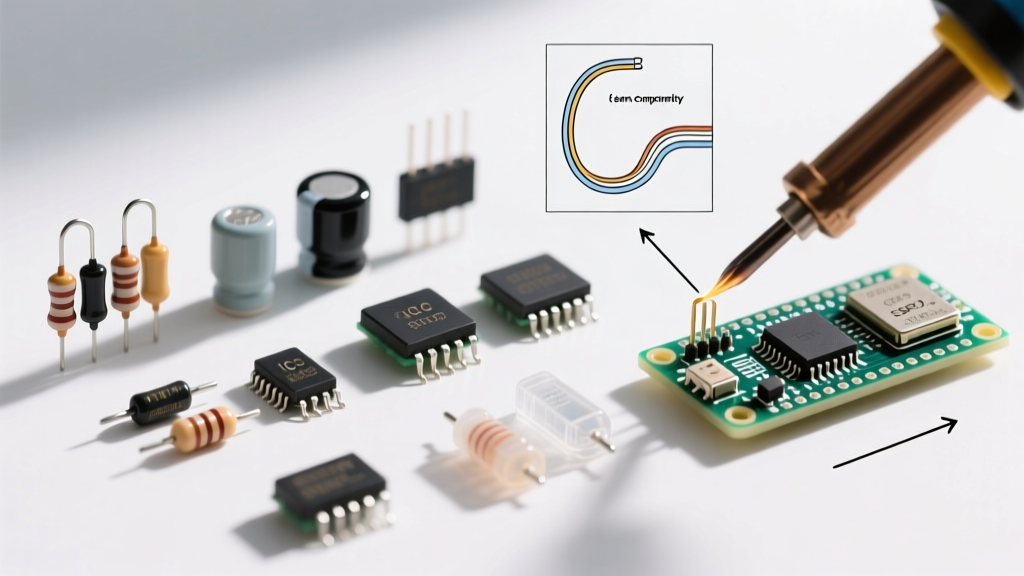
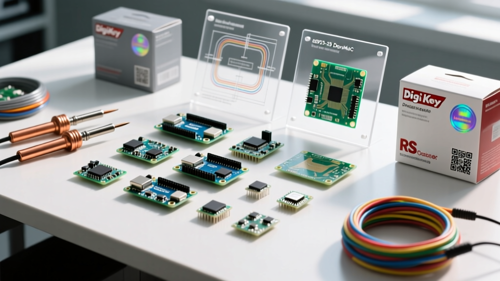
The process begins in the EDA (Electronic Design Automation) software. Whether students are using KiCad, Altium, or Autodesk Fusion Electronics, the lab manager must export a normalized CSV BOM. Using tools like Digi-Key’s BOM Manager or the Octopart API, the manager maps student-chosen generic footprints to specific, in-stock manufacturer part numbers (MPNs). This step prevents the common student error of specifying a 0603 footprint but selecting a through-hole component in their mental model.
2. Verification with Smart Tools
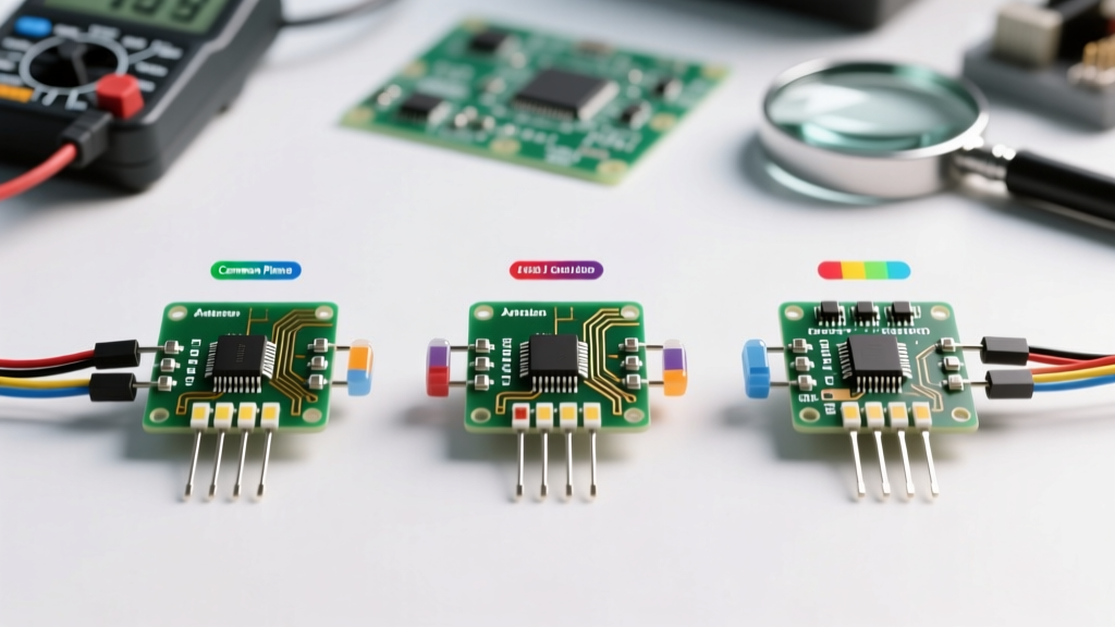
Before bagging, passive components—especially surface-mount device (SMD) capacitors and inductors which lack visual markings—must be verified. Lab technicians use smart tweezers, such as the Elite T320 Smart Tweezers (retailing around $120), to apply a 1kHz test signal and verify capacitance and ESR (Equivalent Series Resistance) on the fly. This catches supplier mislabeling errors before they reach the student's breadboard.
3. ESD-Safe Sorting and Packaging
Static-sensitive components like MOSFETs (e.g., the ubiquitous 2N7000 or IRLZ44N) and modern CMOS logic ICs require strict handling. The ESD Association guidelines mandate that sensitive components be stored and transported in shielding materials. Labs should use 4-mil thick, metal-in anti-static zip bags (such as Uline S-1214, costing roughly $0.14 per bag). Components are sorted on a grounded, dissipative mat before sealing.
4. Thermal Labeling and Traceability
A kit is only useful if its contents are instantly identifiable. Hand-written labels lead to ambiguity (is that '10k' or '100k'?). Professional labs use Bluetooth-enabled thermal transfer printers like the Brother PT-P710BT ($135) to print durable, barcode-scannable labels featuring the MPN, exact value, and a QR code linking to the component's datasheet.
Cost and Time Matrix: Loose Bins vs. Kitted Workflows
Many lab managers resist kitting due to perceived upfront costs. However, when factoring in component loss, student debugging time, and equipment damage, kitting is overwhelmingly more economical. Below is a comparative analysis based on a 30-student cohort building a mixed-signal IoT sensor node (approximate BOM cost: $18.50 per student).
| Metric | Shared Loose Bin Method | Pre-Kitted PBL Workflow |
|---|---|---|
| Lab Prep Time (per cohort) | 1.5 hours (restocking bins) | 4.0 hours (BOM sorting & bagging) |
| Student 'Hunt Time' (per session) | 35 - 45 minutes | 2 - 5 minutes |
| Component Attrition/Loss Rate | 18% (dropped, lost, misfiled) | < 2% |
| Debugging Time (wrong parts) | 2.5 hours avg. per student | 0.5 hours avg. per student |
| ESD Damage Incidents | High (uncontrolled handling) | Negligible (shielded bags) |
| Estimated Hidden Cost per Student | $12.00 (wasted time & broken ICs) | $2.50 (packaging & labeling) |
Critical Failure Modes in Student Kitting
Even when kits are provided, educators must design the BOM and the lab instructions to guard against specific, predictable failure modes that derail PBL outcomes.
- Tolerance Stacking in ADC Dividers: Students frequently substitute 5% carbon-film resistors for 1% metal-film resistors when building voltage dividers for microcontroller ADC inputs. A pre-kitted workflow forces the BOM to specify 1% tolerance (e.g., Yageo MFR-25FBF52-10K), ensuring the analog readings match their theoretical calculations.
- The Counterfeit Voltage Regulator Trap: When students or underfunded labs source components from unauthorized marketplaces to save pennies, they often receive counterfeit LM317 or LM7805 voltage regulators. These fakes lack internal thermal shutdown and over-current protection, leading to catastrophic PCB meltdowns during testing. Kitting from authorized distributors (Mouser, Digi-Key, Arrow) guarantees silicon traceability.
- Gate Punch-Through on MOSFETs: Students often handle bare MOSFETs with dry hands in low-humidity winter environments, generating upwards of 3,000V of static charge. Without the dielectric shielding of proper anti-static bags, the thin gate oxide of a small-signal MOSFET is instantly punctured, resulting in a component that measures fine on a multimeter's diode mode but fails completely under load.
- Polarity Ambiguity on Electrolytic Capacitors: Reversing a polarized aluminum electrolytic capacitor during assembly can cause venting or explosion. Kitting protocols should include a physical visual aid in the bag—a small printed card showing the capacitor's stripe denoting the negative lead, mapped directly to the silkscreen on the student's PCB.
Aligning Kitting with Accreditation Standards
Beyond mere convenience, structured kitting supports rigorous educational standards. The ABET accreditation standards for engineering programs emphasize the ability of students to 'function effectively on a team' and 'develop and conduct appropriate experimentation.' When lab time is not squandered on logistics and faulty parts, student teams can dedicate their hours to iterative testing, data analysis, and design refinement—the exact competencies ABET evaluators look for during program reviews.
Recommended Infrastructure for 2026 STEM Labs
To establish a robust electronic component kitting station, lab managers should allocate a one-time capital budget of approximately $450 to $600. This includes:
- ESD Workstation: A 24x36 inch dissipative rubber mat ($45) with a 1-megohm ground cord connected to a verified earth ground.
- Smart Tweezers: For rapid verification of unmarked SMD passives ($120).
- Labeling System: Brother PT-P710BT or similar industrial thermal printer ($135) with continuous laminated tape.
- Storage & Packaging: Bulk orders of 4-mil metal-in ESD bags and Takachi SW-200 plastic project cases ($3.50 each) for students to store their kits between lab sessions.
By treating electronic component kitting not as a mere administrative chore, but as a foundational element of the pedagogical strategy, educators can drastically elevate the quality, safety, and success rate of their project-based learning environments.