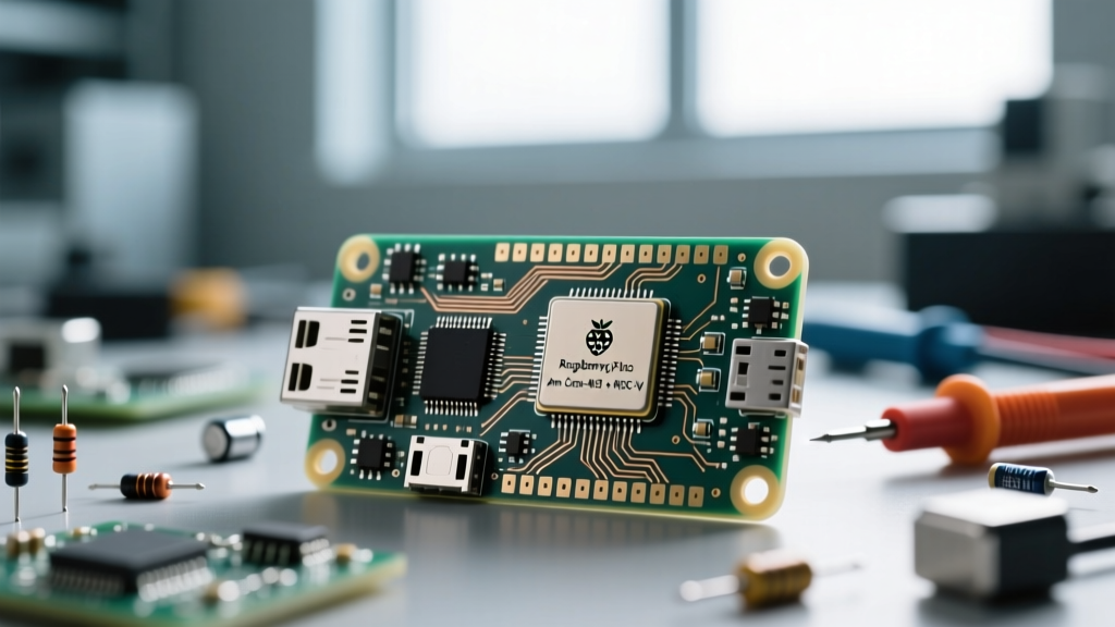

The release of the Raspberry Pi Pico 2 marks a paradigm shift in the microcontroller landscape. While the original RP2040 won hearts with its accessibility and Programmable I/O (PIO), the RP2350 chip powering the Pico 2 introduces a level of architectural complexity and silicon security previously unseen in the sub-$5 hobbyist market. For electrical engineers, embedded developers, and advanced DIYers, the Pico 2 is not just a simple clock-speed bump; it is a fundamental reimagining of what a microcontroller can be.
The Silicon Heartbeat: Inside the RP2350 Architecture
The most headline-grabbing feature of the RP2350 is its heterogeneous dual-architecture design. Unlike traditional MCUs that lock you into a single instruction set, the RP2350 houses two completely different dual-core pairs: a dual-core Arm Cortex-M33 running at 150MHz, and a dual-core Hazard3 RISC-V system also running at 150MHz. However, you cannot run both architectures simultaneously. Instead, the chip's bootrom presents a selection menu upon startup, allowing the developer to choose which core pair will execute the firmware.
The Arm Cortex-M33 is a massive upgrade over the Cortex-M0+ found in the RP2040. Crucially, the M33 includes a single-precision Floating Point Unit (FPU) and Digital Signal Processing (DSP) extensions. This means complex mathematical operations, audio processing, and sensor filtering can now be executed in hardware rather than relying on inefficient software emulation.
On the other side of the silicon sits the Hazard3, a custom open-source RISC-V core designed by Luke Wren. Supporting the RV32IMACZicsr_Zifencei instruction set, the Hazard3 core is a testament to the growing viability of RISC-V in commercial embedded systems. Developers can leverage the Hazard3 GitHub repository to study the exact RTL implementation of the core, a level of transparency that is virtually nonexistent with proprietary silicon vendors.
Memory, Security, and the TrustZone Advantage
Memory constraints often dictate the feasibility of an embedded project. The RP2350 addresses this by expanding the internal SRAM to 520KB. However, this memory is not a single contiguous block; it is divided into four 128KB banks and one 16KB bank. Understanding this banking structure is critical for optimizing DMA (Direct Memory Access) transfers and avoiding bus contention when both cores are hammering the memory controller simultaneously.
Where the Pico 2 truly separates itself from its predecessor—and from competitors like the STM32 or ESP32—is its enterprise-grade security subsystem. The RP2350 integrates Arm TrustZone, secure boot capabilities, and a 16-Kilobit One-Time Programmable (OTP) memory bank.
Warning: The OTP memory is exactly what it sounds like. If you are experimenting with Secure Boot and incorrectly flash your cryptographic keys or lock out the debug interfaces via the OTP, your Raspberry Pi Pico 2 will become a permanent, unrecoverable brick. Always test secure boot configurations on a dedicated sacrificial board before deploying to production hardware.
This security architecture makes the Pico 2 a viable candidate for commercial IoT deployments, point-of-sale terminals, and secure access controllers, where firmware extraction and reverse engineering must be actively prevented.
Pinout Realities and Peripheral Upgrades
While the physical footprint of the Pico 2 module remains identical to the original Pico (featuring 26 exposed castellated GPIO pins), the underlying silicon actually supports up to 48 GPIOs. The remaining pins are accessible only if you design a custom PCB using the raw RP2350 QFN-60 package.
The peripheral suite has received significant attention in the official RP2350 datasheet. The Programmable I/O (PIO) system has been upgraded to PIO v2. While the original PIO was revolutionary for bit-banging protocols like WS2812B LEDs or VGA outputs, PIO v2 introduces direct DMA integration and improved IRQ routing. State machines can now trigger DMA transfers without CPU intervention, drastically reducing jitter in high-speed data acquisition tasks.
Furthermore, the Analog-to-Digital Converter (ADC) has been upgraded to a 12-bit SAR (Successive Approximation Register) architecture. The RP2040 was notorious for ADC noise, particularly on GPIO29 (used for VSYS monitoring). While the RP2350 features improved analog routing and a dedicated temperature sensor pin, hardware designers must still employ strict PCB layout rules—such as isolating analog ground planes and using dedicated LDOs for the ADC VREF—to achieve true 12-bit accuracy.
Pico 2 vs. Pico 1: Is the Upgrade Justified?
For engineers deciding between the legacy Pico 1 and the new Pico 2, the decision hinges on specific project requirements. Below is a technical comparison to aid in platform selection.
| Feature | Raspberry Pi Pico 1 (RP2040) | Raspberry Pi Pico 2 (RP2350) |
|---|---|---|
| Core Architecture | Dual Cortex-M0+ (133MHz) | Dual Cortex-M33 OR Dual Hazard3 RISC-V (150MHz) |
| FPU / DSP | No (Software emulation only) | Yes (Hardware single-precision FPU & DSP) |
| Internal SRAM | 264KB | 520KB (Banked) |
| External Flash | 2MB QSPI | 4MB QSPI (8MB on Pico 2 W) |
| Security | None | Arm TrustZone, Secure Boot, OTP |
| PIO Version | PIO v1 (No direct DMA) | PIO v2 (Direct DMA, enhanced IRQs) |
| ADC Resolution | 12-bit (High noise floor) | 12-bit (Improved SNR, dedicated temp pin) |
| Base Price | $4.00 | $5.00 |
Real-World Gotchas and Hardware Design Rules
Working with the Raspberry Pi Pico 2 in a professional or advanced DIY capacity requires navigating a few modern engineering gotchas. The first is the RISC-V toolchain maturity. While the Arm Cortex-M33 is fully supported by standard CMSIS packs, Keil, and GCC, the Hazard3 RISC-V ecosystem is still maturing. Debugging RISC-V cores via OpenOCD can sometimes yield cryptic halt states, and developers should expect to spend extra time configuring their IDE for RISC-V hardware breakpoints.
The second major consideration is power consumption in battery-operated designs. The RP2350 introduces advanced sleep and dormant modes. In 'Dormant' mode, the core voltage is gated, and the system waits for an external GPIO interrupt or RTC alarm to wake. However, to achieve the microamp-level sleep currents advertised in the datasheet, you must physically disable the onboard switching regulator (if using the Pico module) or design your custom PCB with ultra-low quiescent current LDOs. The Pico 2 module's onboard components will otherwise bleed several milliamps, ruining months-long battery life expectations.
Navigating the Wireless Variant (Pico 2 W)
For IoT applications, the Pico 2 W integrates the Infineon CYW43439 Wi-Fi and Bluetooth LE chip. Unlike the ESP32, which shares its main bus with the radio, the RP2350 communicates with the CYW43439 via a dedicated SPI interface. A critical design rule here is to ensure that your firmware properly manages the SPI bus arbitration between the wireless chip and any external SPI peripherals (like an SD card or external flash). Failing to implement strict mutex locks in your RTOS or FreeRTOS environment will result in corrupted packets and intermittent Wi-Fi drops.
Ultimately, the Raspberry Pi Pico 2 is a masterclass in silicon design. By bridging the gap between hobbyist accessibility and enterprise-grade security, while simultaneously offering a choice between Arm and RISC-V, the RP2350 cements its place as the definitive microcontroller platform for the next generation of embedded electronics.