
Decoding the Arduino Nano Pinout: Beyond the Basics
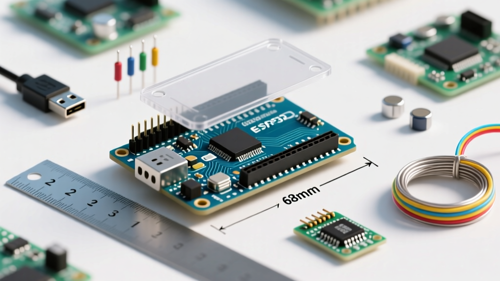
When engineers and makers search for a pinout arduino nano diagram, they are usually met with generic color-coded charts that fail to explain the underlying hardware realities. The Arduino Nano remains one of the most ubiquitous microcontroller boards in the DIY and prototyping space, largely due to its compact 18 x 45 mm footprint and breadboard-friendly layout. However, treating the Nano as just a 'smaller Uno' is a fast track to hardware failure.
In 2026, the market is flooded with both official Arduino Nano boards (priced around $24.50) and high-quality third-party clones featuring USB-C and the CH340C serial chip (typically $4.50 to $6.00). Regardless of the silicon origin, understanding the exact electrical characteristics, multiplexing traps, and power delivery limits of the ATmega328P is critical. This deep dive bypasses the fluff and examines the real-world edge cases of the Nano's pinout.
Power Delivery Architecture: VIN, 5V, and the LDO Trap
The power pins on the Nano are a frequent source of catastrophic failure for intermediate builders. The board features three primary power input methods, each with strict electrical boundaries.
- USB (Mini-USB or Type-C on clones): Provides 5V directly from the host. Protected by a 500mA resettable polyfuse (PTC) and a Schottky diode (typically MBR0520) to prevent backfeeding into the USB port.
- VIN Pin: Accepts 7V to 12V (recommended). This routes through the onboard NCP1117-5.0 linear voltage regulator.
- 5V Pin: Directly taps the 5V logic rail. Bypasses the regulator entirely.
⚠️ Critical Edge Case: The VIN Thermal Bottleneck
If you connect a 12V power supply to the VIN pin and draw 150mA for a sensor array, the NCP1117 LDO must dissipate 1.05W of heat ((12V - 5V) * 0.15A). The Nano's PCB copper pour is insufficient for this thermal load, leading to thermal shutdown at ~150°C. Actionable Advice: If your project draws more than 50mA, bypass the VIN pin. Use a buck converter to step your external voltage down to 5V, and inject it directly into the 5V pin.
Digital I/O, PWM Frequencies, and the Pin 13 Anomaly
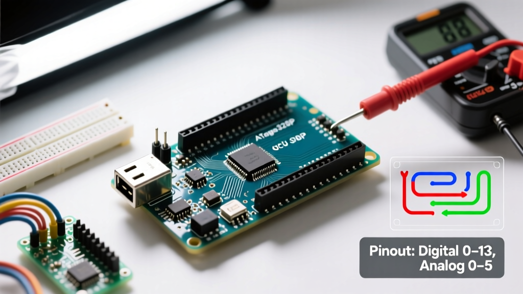
The ATmega328P offers 14 digital I/O pins (D0 to D13). Six of these support hardware Pulse Width Modulation (PWM), denoted by the tilde (~) symbol on the silkscreen: D3, D5, D6, D9, D10, and D11.
According to the Microchip ATmega328P datasheet, the default PWM frequency is approximately 490Hz for most pins, but D5 and D6 operate at 980Hz. This is a vital detail when designing audio filters or driving DC motors where a higher base frequency prevents audible whining.
The Pin 13 Hardware Trap
Pin 13 (SCK for SPI) is wired to an onboard status LED. On older Nano revisions, this was a simple 1kΩ resistor and an LED. On modern official boards, it is driven by an op-amp buffer to isolate the pin. However, on many cheap clones, the LED is still directly tied to the pin via a low-value resistor. If you use Pin 13 as a strict digital input with an external pull-up, the onboard LED circuit will create a voltage divider, preventing the pin from ever reading a clean HIGH. Always test Pin 13 input impedance with a multimeter before finalizing your SPI slave-select routing.
Analog Inputs: The A6 and A7 Beginner Trap
The Nano provides 8 analog input pins (A0 to A7), mapped to the ATmega328P's internal 10-bit ADC. However, the official Arduino Nano hardware documentation explicitly notes a hardware limitation that catches thousands of developers off guard:
Pins A6 and A7 are strictly analog inputs.
Unlike A0 through A5, which are multiplexed with digital I/O ports (PC0-PC5), A6 and A7 are dedicated ADC channels hardwired directly to the analog multiplexer inside the silicon. They lack digital input buffers and output latches.
digitalRead(A6)will fail to compile or return garbage data.digitalWrite(A7, HIGH)will result in a compilation error.- Solution: If you need to read a digital button state, use A0-A5. Reserve A6 and A7 exclusively for potentiometers, LDRs, and analog sensors.
Communication Interfaces: SPI, I2C, and UART Mapping
Routing communication protocols on the Nano requires careful pin management, especially since the board lacks dedicated secondary hardware interfaces (unlike the Arduino Mega).
| Protocol | Function | Nano Pin | ATmega328P Port | Hardware Notes & Edge Cases |
|---|---|---|---|---|
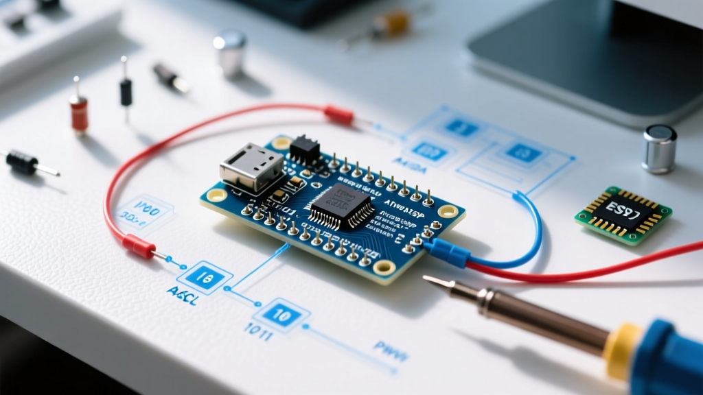
| I2C | SDA | A4 | PC4 | No onboard pull-ups. 4.7kΩ external pull-ups to 5V are mandatory for traces >5cm. |
| I2C | SCL | A5 | PC5 | Shared with ADC. Disable internal pull-ups in code if using as analog. |
| SPI | MOSI | D11 | PB3 | Standard hardware SPI. Do not use SoftwareSPI on these pins. |
| SPI | MISO | D12 | PB4 | Standard hardware SPI. |
| SPI | SCK | D13 | PB5 | Interferes with onboard LED. Use D8 for Software SPI if D13 is compromised. |
| SPI | SS (Slave Select) | D10 | PB2 | Must be set as OUTPUT to keep ATmega in SPI Master mode. |
| UART | TX | D1 | PD1 | Shared with USB-to-Serial bridge (CH340/FT232). Disconnect external TX during USB upload. |
| UART | RX | D0 | PD0 | Shared with USB bridge. 1kΩ series resistor recommended for external RX devices. |
Arduino Nano Every vs. Classic Nano: Pinout Compatibility
As supply chains evolved, Arduino introduced the Nano Every, powered by the ATmega4809. While it shares the exact same physical footprint and silkscreen pinout as the classic ATmega328P Nano, the internal routing differs drastically.
- I2C Multiplexing: On the Classic Nano, I2C is strictly bound to A4/A5. On the Nano Every, the TWI (I2C) peripheral can be remapped to alternate pins via the PORTMUX register, offering massive flexibility for custom PCBs.
- Analog Resolution: The ATmega4809 features a 12-bit ADC (compared to the 328P's 10-bit), but the default Arduino core still returns 10-bit values (0-1023) for backward compatibility. You must use
analogReadResolution(12)to unlock the full 0-4095 range. - 5V Tolerance: The ATmega4809 is natively a 3.3V/5V device, but its absolute maximum ratings on I/O pins are slightly tighter than the legendary ruggedness of the ATmega328P. Never hot-swap 5V inductive loads directly to the Nano Every's I/O without flyback diodes.
Real-World Troubleshooting: The USB Bridge Conflict
A persistent issue in the Nano ecosystem involves the D0 (RX) and D1 (TX) pins. Because the hardware UART is shared with the USB-to-Serial converter (FT232RL on legacy official boards, CH340G/C on modern clones), connecting external modules like Bluetooth HC-05 or GPS NEO-6M directly to D0/D1 causes upload failures.
The Hardware Fix: If you must use hardware UART for an external module, wire the external module's TX pin to the Nano's RX (D0) through a 1kΩ series resistor. This allows the USB bridge's TX signal to overpower the external module's TX signal during firmware uploads, preventing the 'avrdude: stk500_recv(): programmer is not responding' error, while still allowing normal serial communication post-boot.
Summary Checklist for Nano Prototyping
- Verify if your clone uses a CH340 or FT232 chip to ensure correct driver installation on Windows/macOS.
- Never use
digitalRead()on A6 or A7. - Inject 5V directly into the 5V pin for high-current servo/LED projects; avoid the VIN LDO.
- Add 4.7kΩ pull-up resistors to A4 and A5 for I2C sensor stability.
- Isolate Pin 13 if using it as a digital input or sensitive SPI clock line.