
The Hidden Boot Sequence: Why Strapping Pins Matter
When designing custom PCBs or wiring breadboards with the ESP32, encountering a boot loop, a silent failure, or the dreaded "Timed out waiting for packet header" error is a common rite of passage. The culprit is almost always a misunderstanding of ESP32 strapping pins. Unlike standard microcontrollers where every GPIO is immediately available for user logic upon power-up, the ESP32 ROM bootloader samples a specific subset of pins during the rising edge of the EN (Reset) signal. These sampled states dictate the chip's boot mode, SPI flash voltage, and debug log routing.
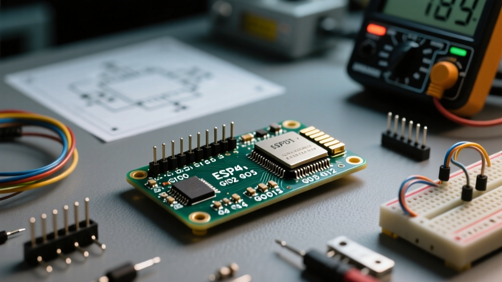
If external circuitry forces these pins into conflicting logic levels during the critical 10-microsecond sampling window, the ESP32 will enter unintended boot modes or fail to initialize the flash memory. This configuration guide provides a deep-dive into ESP32 strapping pins GPIO0, GPIO2, GPIO4, GPIO5, GPIO12, and GPIO15, equipping you with the hardware design rules required for stable MCU startups.
Complete Breakdown: ESP32 Strapping Pins GPIO0, GPIO2, GPIO4, GPIO5, GPIO12, GPIO15
GPIO0 & GPIO2: The Boot Mode Selectors
The primary boot mode is determined by the interplay between GPIO0 and GPIO2. By default, the ESP32 is designed to boot from the external SPI flash. However, if you need to flash new firmware via UART, you must manipulate these pins.
- GPIO0: Features an internal weak pull-up resistor during reset. If left floating or pulled HIGH, the chip boots from SPI Flash. If pulled LOW (typically via a tactile "BOOT" button), the chip enters the UART Serial Download Mode.
- GPIO2: Features an internal weak pull-down resistor. For a successful SPI Flash boot, GPIO2 must be LOW or floating. If pulled HIGH, the ROM bootloader attempts an SDIO boot, which will fail on standard WROOM/WROVER modules and result in a continuous boot loop.
GPIO12 (MTDI): SPI Flash Voltage Configuration
GPIO12 is arguably the most dangerous strapping pin for custom hardware designers. It dictates the voltage regulator output for the external SPI flash chip.
According to the Espressif ESP32 Datasheet, if GPIO12 is pulled HIGH during reset, the internal LDO configures the flash VDD to 1.8V. If LOW or floating, it defaults to 3.3V.
If you are using a standard 3.3V flash module (like the Winbond W25Q32) but an external sensor circuit pulls GPIO12 HIGH during boot, the ESP32 will under-volt the flash. This causes immediate brownouts, corrupted flash reads, and the infamous "flash read err, 1000" panic message in the serial monitor.
GPIO15 (MTDO): Boot Log & JTAG Routing
GPIO15 controls the routing of the boot loader debug logs and JTAG signals. It has an internal pull-up. When HIGH (default), boot logs are output to UART0 (GPIO1/GPIO3). When pulled LOW, logs are routed to UART1 or SDIO pins. For 99% of DIY and commercial applications, GPIO15 should be left floating or pulled HIGH to ensure you can read serial monitor outputs during debugging.
GPIO5 & GPIO4: Secondary Timing and SDIO Configs
While GPIO0, 2, 12, and 15 handle the primary boot matrix, GPIO5 and GPIO4 play secondary roles in specific configurations.
- GPIO5: Often used in conjunction with GPIO0 to configure SPI flash timing and SDIO slave modes. In standard SPI boot, it should generally be left unforced to allow the ROM bootloader to set default SPI clock timings.
- GPIO4: Tied to the SDIO boot matrix and JTAG enablement. If you are not utilizing the ESP32 as an SDIO slave or using advanced JTAG debugging, GPIO4 is safe to use as a standard input/output post-boot, provided it is not driven externally during the reset phase.
The EN Pin Timing & RC Capture Window
The strapping pins are not sampled continuously; they are sampled exactly once during the rising edge of the EN (Chip Enable) pin. In most custom PCB designs, the EN pin is tied to VCC via a 10kΩ resistor and a 100nF capacitor to ground to prevent brownout resets. This RC network creates a slow voltage ramp. According to the Espressif Hardware Design Guidelines, the EN pin must reach the VIH threshold cleanly. If your external strapping pin circuits have large capacitive loads, they may not settle to their final logic HIGH or LOW states before the EN pin crosses the sampling threshold. Always ensure that any external pull-up or pull-down resistors on strapping pins are strong enough (typically 4.7kΩ to 10kΩ) to overcome parasitic capacitance within the first few microseconds of the EN ramp.
Wiring Matrix: Safe States for Custom PCB Design
When designing your schematic, use this matrix to ensure your external components do not interfere with the reset sampling window. Always use series resistors or RC delay circuits if a peripheral must share a strapping pin.
| Strapping Pin | Internal State at Reset | Required State for Normal SPI Boot | Common Hardware Conflict |
|---|---|---|---|
| GPIO0 | Pull-Up | HIGH or Floating | I2C devices pulling SDA/SCL low |
| GPIO2 | Pull-Down | LOW or Floating | Onboard LEDs or external pull-ups |
| GPIO4 | Pull-Down | LOW or Floating | Active-high relays or MOSFET gates |
| GPIO5 | Pull-Up | HIGH or Floating | Active-low chip select lines |
| GPIO12 | Pull-Down | LOW or Floating (for 3.3V Flash) | Sensors with default HIGH outputs |
| GPIO15 | Pull-Up | HIGH or Floating | Active-low enable pins on peripherals |
Real-World Failure Modes & Troubleshooting
The GPIO2 LED Trap
Many development boards feature a built-in LED connected to GPIO2. If you add an external pull-up resistor to this pin to make the LED brighter, or if you wire an active-high component to it, the ESP32 will fail to boot. Solution: If you must drive a load on GPIO2, use an N-channel MOSFET where the ESP32 pin drives the gate through a 100Ω series resistor, ensuring the pin remains low-impedance to ground during reset.
The GPIO12 Relay Brownout
A classic mistake in home automation PCBs is wiring a relay control transistor directly to GPIO12. If the base-emitter junction or a pull-up network inadvertently pulls GPIO12 above the 0.7V threshold during the EN rising edge, the ESP32 switches to 1.8V flash mode. Solution: Add a 10kΩ pull-down resistor to GPIO12, or better yet, move the relay control to a non-strapping pin like GPIO26 or GPIO27.
Oscilloscope Debugging for Boot Failures
When a board fails to boot, connect a 4-channel oscilloscope to EN, GPIO0, GPIO2, and GPIO12. Trigger on the rising edge of EN. You should observe the strapping pins settling to their target voltages at least 5 microseconds before EN crosses the ~0.75V logic threshold. If GPIO12 shows a slow ramp that crosses 0.5V right as EN triggers, the internal sampler may read it as an indeterminate state, leading to randomized boot failures that only occur when the board is warm or when humidity changes the parasitic capacitance.
Overriding Strapping States in Firmware via eFuse
If you have already manufactured a PCB and discovered that GPIO12 is permanently pulled HIGH by an unavoidable sensor circuit, your board will continuously brownout the 3.3V flash. Fortunately, the ESP-IDF Bootloader Documentation details a hardware-level override using the ESP32's eFuses.
You can permanently force the ESP32 to use 3.3V for the flash, ignoring the GPIO12 strapping state, by burning the XPD_SDIO_FORCE, XPD_SDIO_REG, and XPD_SDIO_TIEH eFuses. Using the espefuse.py tool provided by Espressif, you can execute the following command via UART:
espefuse.py set_flash_voltage 3.3VWarning: eFuse burning is a one-time irreversible physical process. Verify your multimeter readings and schematic logic before executing this command.
Authoritative References & Further Reading
To ensure your designs comply with official RF and digital layout requirements, always cross-reference your schematics with official documentation. Proper decoupling capacitor placement near the EN pin is just as critical as strapping pin management, as a noisy EN rising edge can cause the ROM bootloader to sample the strapping pins before external RC circuits have settled into their final logic states.