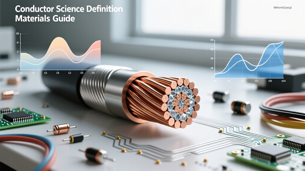

The Core Conductor in Science Definition: Beyond Basic Textbooks
When students first encounter electricity, they are often given a simplified explanation of materials that allow current to flow. However, the rigorous conductor in science definition requires a deeper dive into quantum mechanics and solid-state physics. In formal scientific terms, a conductor is a material that permits the macroscopic flow of electric charge carriers—typically electrons, but occasionally ions or holes—when subjected to an electric field. Unlike insulators, which tightly bind their valence electrons to individual atoms, conductors possess a lattice structure that supports a 'sea' of delocalized electrons capable of moving freely through the material.
For electrical engineers, DIY electronics enthusiasts, and wire sizing specialists, understanding this fundamental physics definition is not merely an academic exercise. It dictates everything from the National Electrical Code (NEC) ampacity tables to the selection of specialized RF coaxial cables. By examining the atomic behavior of conductive materials, we can predict voltage drop, thermal dissipation, and long-term termination reliability.
Energy Band Theory: Why Some Materials Conduct and Others Insulate
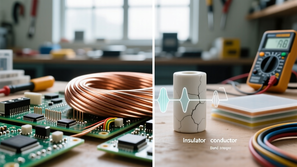
To truly grasp the conductor in science definition, one must look at Energy Band Theory. In solid-state physics, the discrete energy levels of individual atoms merge into continuous 'bands' when atoms bond to form a solid lattice. The two most critical bands for electrical conduction are the valence band (the highest energy range occupied by electrons at absolute zero) and the conduction band (the range of electron energies higher than the valence band, where electrons are free to move).
According to resources from Georgia State University's HyperPhysics, the distinction between conductors, semiconductors, and insulators lies entirely in the 'band gap' between these two regions:
- Conductors: The valence band and conduction band overlap. There is zero band gap. Even at room temperature, thermal energy is sufficient to promote vast numbers of electrons into the conduction band, allowing immediate current flow.
- Semiconductors: A small band gap exists (typically 0.1 to 2.5 eV). Electrons require external energy (heat, light, or voltage) to jump the gap.
- Insulators: A massive band gap (greater than 4 eV) prevents electrons from reaching the conduction band under normal conditions.
Metals like copper, silver, and aluminum naturally exhibit this overlapping band structure, making them the foundational elements of all modern wiring systems.
Reference Chart: Electrical Conductivity of Common Elements & Alloys
When sizing wires or designing printed circuit boards (PCBs), referencing the exact electrical conductivity of materials is vital. The standard metric for this is the International Annealed Copper Standard (% IACS), where pure, annealed copper at 20°C is defined as exactly 100% IACS (equivalent to 58.0 MS/m, though modern high-purity copper often tests slightly higher).
| Material | Conductivity (MS/m at 20°C) | % IACS | Primary Engineering Use Case |
|---|---|---|---|
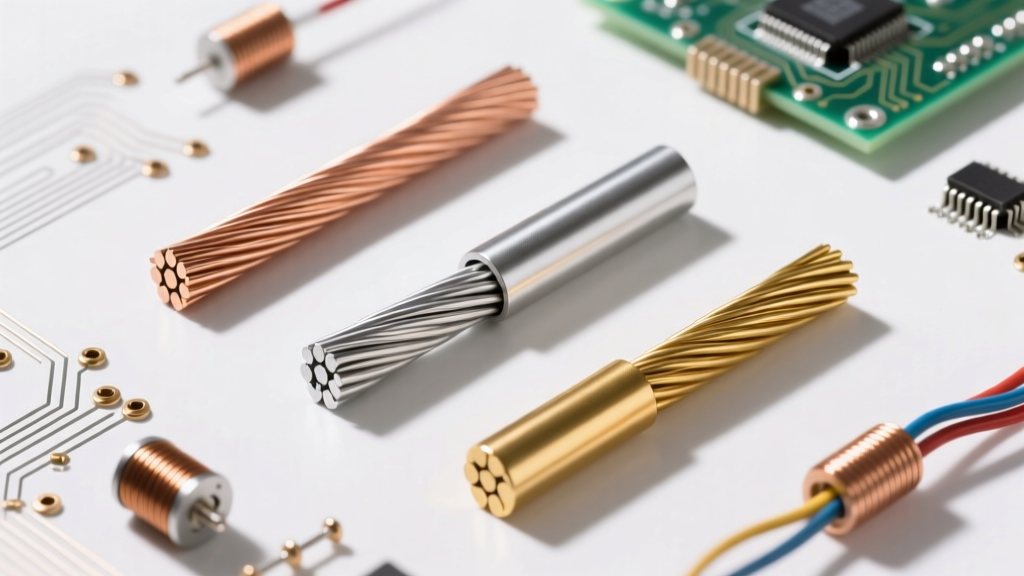
| Silver (Ag) | 63.0 | 105% | RF contacts, high-end audio switches, aerospace relays |
| Copper (Cu) | 59.6 | 100% | Standard branch circuit wiring, PCB traces, motor windings |
| Gold (Au) | 45.5 | 76% | Corrosion-resistant edge connectors, microelectronics bonding |
| Aluminum (Al) | 35.8 | 61% | High-voltage overhead transmission lines, large feeder cables |
| Tungsten (W) | 18.9 | 31% | Incandescent filaments, high-temperature vacuum environments |
While silver holds the crown for bulk electrical conductivity, copper remains the undisputed champion of practical electrical engineering due to its optimal balance of cost, tensile strength, and predictable oxidation characteristics.
Thermal vs. Electrical Conduction: The Wiedemann-Franz Law
A crucial, often overlooked aspect of the conductor in science definition is the intrinsic link between electrical and thermal conductivity. The Wiedemann-Franz Law states that the ratio of the thermal conductivity to the electrical conductivity of a metal is directly proportional to the absolute temperature.
Because the same free electrons are responsible for transporting both electric charge and thermal energy, materials that are excellent electrical conductors are almost universally excellent heat conductors. Data compiled by the National Institute of Standards and Technology (NIST) consistently reinforces this physical coupling across metallic elements.
For DIY electronics and wire sizing, this scientific law has massive practical implications. A copper wire that exhibits high resistance due to poor termination will not only suffer from voltage drop but will also efficiently transfer the resulting heat back toward the breaker panel or the sensitive microcontroller pins. This is why high-amperage ESCs (Electronic Speed Controllers) in RC models and drones utilize thick silicone-insulated copper wire and massive aluminum heat sinks—the thermal conduction properties are just as vital as the electrical ones.
High-Frequency Conduction: The Skin Effect Phenomenon
The classical definition of a conductor assumes Direct Current (DC) or low-frequency Alternating Current (AC), where charge carriers utilize the entire cross-sectional area of the wire. However, as frequency increases, electromagnetism alters the conductor's behavior through the Skin Effect.
At high frequencies, changing magnetic fields induce eddy currents within the conductor that oppose the flow of electrons in the center of the wire. Consequently, the current is forced to the outer 'skin' of the conductor. The skin depth is the distance from the surface where the current density falls to 37% of its surface value.
- At 60 Hz (Mains Power): The skin depth in copper is roughly 8.5 mm. Standard 12 AWG wire (1.02 mm radius) is fully utilized.
- At 1 MHz (RF/AM Radio): The skin depth shrinks to approximately 0.066 mm. The center of a standard wire becomes electrically dead weight.
This scientific reality forces RF engineers to use specialized conductors. Litz wire (comprising hundreds of individually insulated micro-strands) or silver-plated copper wires are utilized to maximize surface area, proving that the physical geometry of the conductor must adapt to the frequency of the charge flow.
Troubleshooting Conductor Degradation: Oxidation, Creep, and Galvanic Action
Understanding the material science behind conductors is essential for troubleshooting real-world electrical failures. The scientific definition of a perfect conductor assumes a flawless crystal lattice, but real-world environments introduce degradation mechanisms.
1. Aluminum Creep and Cold Flow
Aluminum is highly susceptible to 'creep'—a slow, permanent deformation under constant mechanical stress. When an aluminum wire is clamped under a standard copper lug screw, the continuous pressure causes the aluminum to yield and flow away from the connection over time. This reduces the contact pressure, increases contact resistance, and generates dangerous heat. Modern NEC codes require specific CO/ALR-rated receptacles and torque-screwdriver verification to combat this material science flaw.
2. Galvanic Corrosion
When two dissimilar conductors (like copper and aluminum) are joined in the presence of an electrolyte (even ambient humidity), a galvanic cell is formed. Aluminum, being more anodic, will rapidly corrode and turn into a powdery aluminum oxide insulator. This is why direct copper-to-aluminum splices require specialized bi-metallic connectors or anti-oxidant pastes like Noalox, which contain zinc dust to intercept the galvanic reaction.
3. Electromigration in Microelectronics
At the microscopic scale of integrated circuits, high current densities can physically strip metal atoms from the conductor lattice and push them down the line, creating voids (open circuits) and hillocks (short circuits). This phenomenon, governed by the momentum transfer from electrons to metal ions, is a primary failure mode in modern microprocessors and a major focus of semiconductor materials science.
Mastering the conductor in science definition bridges the gap between abstract quantum physics and the physical act of stripping, terminating, and sizing wires. Whether you are calculating the voltage drop for a 200-amp residential service or designing a high-frequency antenna, respecting the atomic and thermodynamic properties of your chosen materials is the hallmark of true electrical expertise.