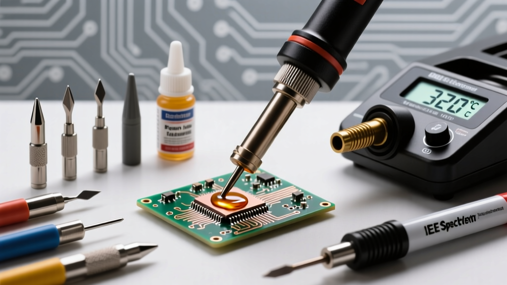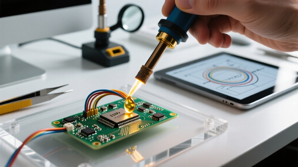

Mastering the Fundamentals of Wire-to-PCB Connections
While surface-mount technology (SMT) dominates modern manufacturing, soldering wire to PCB board assemblies remains a critical skill for prototyping, high-current power delivery, and field repairs. According to the IPC J-STD-001 standard for soldered electrical and electronic assemblies, a reliable wire termination must exhibit proper wetting, a smooth concave fillet, and zero evidence of thermal damage to the substrate. Yet, this seemingly simple task is a leading cause of field failures due to mechanical stress, solder wicking, and lifted pads.
In this comprehensive guide, we break down the safety protocols, material selections, and precise thermal techniques required to create bulletproof wire-to-PCB joints in 2026, whether you are using a budget-friendly Pinecil V2 or a professional Hakko FX-951 station.
Essential Safety Gear and Workspace Setup
Before picking up your iron, establishing a safe environment is non-negotiable. Soldering generates particulate matter and volatile organic compounds (VOCs) from flux activation.
- Fume Extraction: Never solder in a stagnant room. Use an active HEPA and carbon-filter fume extractor. The Cornell University Environmental Health and Safety guidelines mandate local exhaust ventilation to capture rosin-based fumes, which are known respiratory sensitizers. A Hakko FA-400 (~$110) or a BOFA AD Oracle system for heavy production are excellent choices.
- ESD Protection: When working on live or sensitive microcontroller boards, use an anti-static mat and a grounded wrist strap to prevent electrostatic discharge from destroying sensitive ICs.
- Lead Hygiene: If you are using traditional Sn63/Pb37 solder, wash your hands thoroughly with cold water and soap immediately after your session. Never eat or drink at your soldering bench.
Choosing the Right Materials for PCB Wire Joints
The reliability of your joint starts before the iron even heats up. Selecting the correct wire gauge, solder alloy, and flux chemistry dictates the mechanical and electrical integrity of the final assembly.
Solder Alloy Comparison Matrix
| Alloy Designation | Composition | Melting Point | Ideal Iron Temp | Best Application |
|---|---|---|---|---|
| Sn63/Pb37 (Eutectic) | 63% Tin, 37% Lead | 183°C (361°F) | 320°C - 340°C | Prototyping, DIY, repair, aerospace |
| SAC305 (Lead-Free) | 96.5% Sn, 3% Ag, 0.5% Cu | 217°C (423°F) | 350°C - 380°C | Commercial production, RoHS compliance |
| Sn60/Pb40 | 60% Tin, 40% Lead | 183°C - 190°C | 320°C - 340°C | General purpose, non-critical joints |
Note: For wire-to-PCB connections, Sn63/Pb37 (like Kester 245) is vastly superior for DIY and repair due to its eutectic nature (instant liquid-to-solid transition), which prevents 'disturbed joints' if the wire moves slightly during cooling.
Wire Preparation and Stripping
Never use dull side-cutters to strip wires; this nicks the copper strands, creating a weak point that will snap under vibration. Use precision thermal wire strippers or calibrated mechanical strippers. Strip exactly 3mm to 5mm of insulation for standard through-hole pads. Stripping too much bare wire invites solder wicking and short-circuit risks.
Step-by-Step: Soldering Wire to PCB Board Safely
Follow this optimized thermal sequence to ensure maximum wetting without delaminating the copper pad from the FR4 substrate.
- Pre-Tin the Wire: Apply a small amount of flux to the stripped wire strands. Touch your tinned iron tip to the wire and feed solder until the strands are fully coated and shine brightly. Do not let solder wick past the insulation jacket.
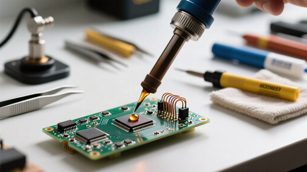
- Pre-Tin the PCB Pad: If the pad is not already tinned, apply a dab of tacky flux (like Amtech NC-559-V2-TF) to the pad. Touch the iron to the pad for 1 second and feed a tiny amount of solder to create a small dome.
- The Marriage (Heat Transfer): Hold the pre-tinned wire flat against the pre-tinned pad. Apply the clean, tinned tip of your soldering iron to both the wire and the pad simultaneously.
- Reflow and Fillet Formation: Within 1 to 2 seconds, the solder on both the wire and the pad will reflow and merge. Feed a microscopic amount of additional solder if needed to form a smooth, concave fillet that covers the wire strands and the pad.
- Remove and Cool: Pull the iron away first, then hold the wire perfectly still for 3-5 seconds until the solder solidifies. Blowing on the joint can cause micro-fractures in lead-free alloys.
The 3-Second Rule: According to NASA Workmanship Standards (NASA-STD-8739.3), the total dwell time of the soldering iron on a PCB pad should rarely exceed 3 to 5 seconds. Prolonged heat exposure breaks down the epoxy bond between the copper trace and the fiberglass substrate, resulting in catastrophic pad lifting.
Mechanical Strain Relief: The Secret to Long-Lasting Joints
A perfect metallurgical bond will still fail if the wire acts as a lever. Every time a cable is tugged, the mechanical stress concentrates exactly at the edge of the solder joint, eventually cracking the fillet or ripping the pad off the board. Strain relief is mandatory for any wire leaving a PCB enclosure.
Effective Strain Relief Methods
- Polyamide Hot Glue: Apply a generous bead of high-temperature hot glue over the solder joint and the first 10mm of the wire insulation. This creates a flexible, shock-absorbing boot that distributes mechanical stress away from the rigid solder joint.
- UV-Curable Solder Mask: For a professional, low-profile finish, apply UV curable conformal coating over the joint and cure it with a 365nm UV flashlight for 60 seconds. This creates a hard, durable shell.
- Kapton Tape & Zip Ties: Route the wire through a nearby mounting hole or secure it to the board with Kapton tape and a small nylon cable tie, ensuring the wire cannot pivot at the solder point.
Common Failure Modes and Troubleshooting
Even experienced technicians encounter issues when soldering wire to PCB board assemblies. Here is how to diagnose and fix them:
- Solder Wicking: Symptom: Solder creeps up the wire under the insulation, making the wire stiff and prone to snapping. Fix: Strip less wire (2mm instead of 5mm), use a lower iron temperature, and pre-tin the wire vertically so gravity prevents upward wicking.
- Cold Joints: Symptom: The solder looks dull, grainy, or forms a convex ball rather than a concave fillet. Fix: Your iron temperature is too low, or you failed to heat the pad adequately. Clean the tip with brass wool (Hakko 599B), increase the temp by 15°C, and ensure the tip touches both the wire and the copper pad.
- Pad Lifting / Delamination: Symptom: The copper pad peels away from the green FR4 board. Fix: This is thermal damage. You held the iron on the pad too long. Use a higher-wattage iron (like a 70W+ station) which recovers heat faster, allowing you to complete the joint in under 2 seconds rather than lingering with a 15W iron that slowly bakes the board.
Frequently Asked Questions (FAQ)
Can I use lead-free solder for wire-to-PCB connections?
Yes, but it requires higher temperatures (360°C+) and aggressive flux. Lead-free alloys like SAC305 do not wet as easily as Sn63/Pb37 and are more prone to disturbed joints if the wire moves during the longer cooling phase. For DIY and repair, leaded eutectic solder remains the gold standard for wire terminations.
Why does my solder refuse to stick to the PCB pad?
Oxidation is the enemy of solder wetting. If the pad is tarnished or covered in old, burnt flux, the new solder will ball up and roll off. Clean the pad with isopropyl alcohol (99%) and a fiberglass scratch pen or apply a generous amount of liquid no-clean flux to break down the oxidation layer before applying heat.
What wire gauge is best for signal vs. power connections?
For low-current logic signals (I2C, SPI, UART), use 26 AWG to 30 AWG silicone stranded wire to minimize pad stress. For power delivery (12V/5V rails drawing 2A+), use 18 AWG to 14 AWG wire, but ensure you are using a high-wattage soldering station (minimum 65W) to provide enough thermal mass to heat the thick copper strands.