
The Anatomy of Wide Tip Failure
When electronics engineers and plumbing technicians refer to a wide soldering iron tip, they are typically describing chisel tips exceeding 4.0mm in width (such as the Hakko T18-D52 or Weller RT4), spade tips, or wide-blade cartridges like the JBC C245-945. These tips are engineered with high thermal mass to transfer joules rapidly into heavy ground planes, thick copper pours, and large-gauge wiring. However, troubleshooting failure wide soldering iron scenarios requires understanding the metallurgical limits of the tip itself.
According to Hakko's Official Tip Care Guidelines, a standard soldering tip consists of a high-conductivity copper core, an electroplated iron layer typically measuring between 100 and 150 microns thick, and a flash-tinned outer coating. The iron layer is the only barrier preventing the molten solder from dissolving the copper core. When wide tips fail, it is almost always due to the breach, oxidation, or thermal fatigue of this microscopic iron shield.
Primary Failure Modes of Wide Soldering Tips
Wide tips experience unique mechanical and thermal stresses compared to fine-point conical tips. Because their surface area is larger, they are often subjected to higher station temperatures by frustrated users attempting to heat massive thermal sinks. Below is a diagnostic matrix for identifying why your wide blade or heavy chisel tip is failing to wet.
| Failure Mode | Visual Symptom | Root Cause | Reversibility |
|---|---|---|---|
| Severe Oxidation | Thick, dark blue/black crust that repels molten solder. | Leaving the iron idle at >350°C without a protective solder blob. | High (if caught early) |
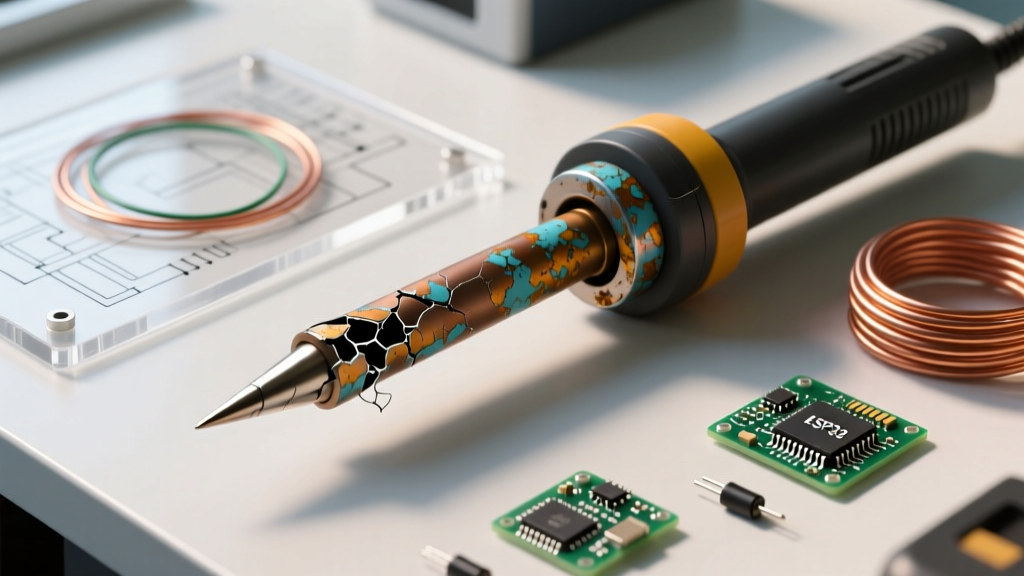
| Iron Plating Dissolution | Pitting, craters, or a bitten appearance on the working face. | Using highly active fluxes or exceeding 390°C with SAC305 lead-free solder. | None (Tip is destroyed) |
| Thermal Fatigue Cracking | Micro-fissures near the base of the wide bevel. | Quenching a hot wide tip in wet sponges or liquid flux. | None (Risk of copper leaching) |
| Carbon Buildup | Black, hardened rosin char on the upper shaft of the tip. | Burning flux vapors due to poor tip-to-heater thermal coupling. | Moderate (Requires chemical cleaning) |
The Thermal Mass Trap: Why Wide Tips Degrade Faster
A common scenario in both DIY and professional settings is the ground plane trap. When attempting to solder a 14AWG wire to a multi-layer PCB ground lug, the massive copper area acts as a heat sink, pulling thermal energy away from the joint faster than the iron can supply it. The amateur response is to crank the soldering station to 420°C or higher.
Expert Insight: The IPC standards body (specifically within J-STD-001 guidelines) heavily discourages excessive dwell times and extreme temperatures. Exceeding 380°C exponentially accelerates the dissolution rate of the iron plating into tin-based solders. A wide tip held at 420°C will lose its 120-micron iron plating in a fraction of the time it would at 340°C, leading to catastrophic copper core exposure.
Furthermore, wide tips suffer from lateral thermal gradients. If the heater core inside the station ceramic element does not make perfect 360-degree contact with the wide tip inner barrel, the working face will run cooler than the sensor reads. The user compensates by turning up the dial, inadvertently overheating the base of the tip and causing the internal copper to oxidize and swell, which permanently ruins the fitment inside the heating element.
Active vs. Passive Wide Tip Architectures
In 2026, the market is split between passive tips (where the heater is in the wand) and active cartridges (where the heater is integrated into the tip). Understanding this distinction is vital for preventing failure:
- Passive Wide Tips (e.g., Hakko T18 series, Weller ETA): Cost-effective ($8 to $12 per tip) but suffer from thermal lag. To prevent failure on heavy joints, you must use a high-wattage station (70W+) to maintain recovery rates without artificially inflating the idle temperature.
- Active Wide Cartridges (e.g., JBC C245, Pace TD200): Expensive ($45 to $65 per cartridge) but feature integrated thermocouples millimeters from the working face. They rarely suffer from thermal fatigue failure because the station cuts power the microsecond the target temperature is reached, eliminating the overshoot that destroys iron plating.
Step-by-Step Recovery Protocol for Oxidized Wide Tips
If your wide chisel or spade tip has turned black and refuses to accept solder, do not immediately discard it or resort to sandpaper. Abrasives will instantly destroy the iron plating. Instead, follow this chemical and thermal recovery protocol endorsed by experts at Adafruit's Excellent Soldering Guide and industrial maintenance teams.
- Drop the Temperature: Lower your station to 250°C. High heat will instantly flash-burn any chemical cleaners you apply.
- Apply Tip Tinner: Press the wide face of the iron firmly into a pot of aggressive tip tinner (such as MG Chemicals 860 or Amtech Tip Tinner). The mixture of phosphoric acid and tin powder will strip the oxidation.
- Wipe on Brass Wool: While the tip is still coated in the molten tinner sludge, wipe it gently in a dry brass wire sponge. Never use a wet cellulose sponge, as the thermal shock on a wide, high-mass tip can cause microscopic cracking.
- Re-Tin Immediately: Apply a thick layer of 63/37 rosin-core solder to the entire working face. The leaded solder will protect the freshly exposed iron layer while the iron idles.
- Repeat if Necessary: For severe crust buildup, you may need to repeat steps 2 through 4 three or four times. If the underlying pitting remains, the iron plating is gone, and the tip must be recycled.
Preventative Maintenance Matrix for Heavy-Duty Tips
Preventing failure in wide soldering iron tips is vastly cheaper than replacing $50 active cartridges or dealing with cold, unreliable joints on critical infrastructure. Implement these specific parameters into your workbench routine:
- The Blob Rule: Always leave a massive, 5mm-thick blob of cheap, leaded 60/40 solder on the wide working face before powering down the station. This sacrificial layer oxidizes instead of the iron plating.
- Use Low-Activity Fluxes: When working with wide tips on large terminals, avoid highly corrosive plumbing acid fluxes unless absolutely necessary. If you must use them, clean the tip with isopropyl alcohol and a brass brush immediately after the joint is made.
- Auto-Sleep is Mandatory: Wide tips hold heat for a long time. If your station lacks an auto-sleep feature that drops the temperature to 150°C after 5 minutes of inactivity, manually turn the dial down. Idling a wide tip at 350°C for just 20 minutes can cause irreversible blue-oxide scaling.
- Match the Tip to the Joint: Do not use a 2mm chisel to heat a 10mm ground pad by holding it there for 15 seconds. The prolonged dwell time will transfer heat up the shaft and cook the internal flux. Use a 6mm spade tip to transfer the heat in 3 seconds, protecting both the tip and the PCB pad.
Conclusion
Troubleshooting wide soldering iron tip failure ultimately comes down to respecting the metallurgical boundaries of the tool. By recognizing the thermal mass trap, avoiding extreme temperature compensation, and utilizing chemical tinning compounds instead of mechanical abrasion, you can extend the lifespan of your heavy-duty chisels and spades from a few weeks to several years. Whether you are soldering thick-gauge automotive wiring or multi-layer RF boards, treating your wide tips with precision will ensure consistent, IPC-compliant joints every time.