
Defining the Process: What Does Soldering Mean at Scale?
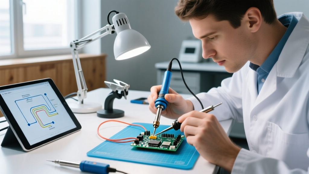
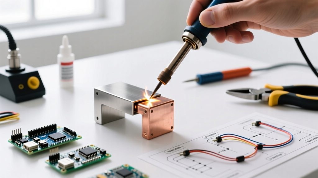
When electronics engineers and manufacturing specialists ask what does soldering mean for high-volume, high-reliability production, the answer extends far beyond simply melting metal to join two components. In the DIY and hobbyist space, soldering is often viewed as a basic mechanical and electrical connection. However, in industrial printed circuit board (PCB) assembly, soldering is a highly controlled metallurgical process. It is the deliberate creation of an Intermetallic Compound (IMC) layer that dictates the long-term survival of electronic systems in harsh environments.
At the industrial level, a solder joint is not merely a glue; it is a complex alloy matrix that must withstand severe thermal cycling, mechanical shock, and continuous electrical current. According to guidelines maintained by the IPC Standards Hub, achieving a reliable joint requires strict adherence to thermal profiles, precise flux chemistry, and exact alloy compositions. Understanding the true definition of industrial soldering is the first step toward optimizing yield rates and ensuring compliance with stringent Class 3 high-reliability standards.
The Metallurgy of the Joint: Intermetallic Compound (IMC) Formation
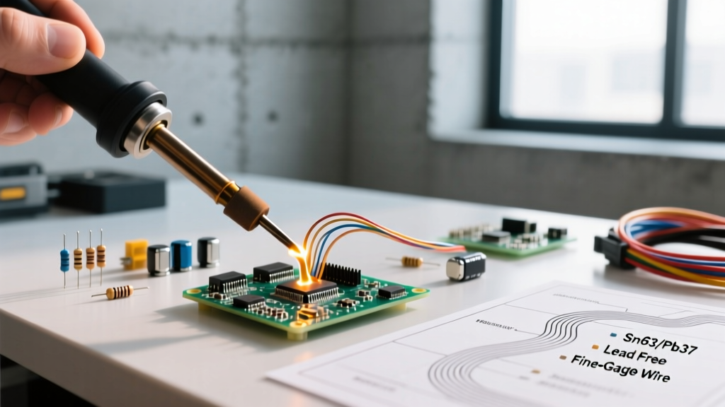
To grasp what soldering means from a materials science perspective, we must look at the microscopic boundary between the solder alloy and the copper pad. When molten solder (typically a Tin-based alloy like SAC305) contacts a copper surface, a metallurgical reaction occurs, forming an IMC layer—primarily Cu6Sn5 (eta phase) and Cu3Sn (epsilon phase).
- Optimal Thickness: A healthy IMC layer should measure between 1.0 and 2.5 micrometers.
- Under-soldering (Cold Joint): If the thermal energy is too low, the IMC layer is incomplete, leading to high electrical resistance and immediate mechanical failure under vibration.
- Over-soldering (Thermal Damage): Excessive heat or prolonged time above liquidus (TAL) causes the IMC layer to grow too thick (over 4.0 micrometers). This makes the joint brittle and highly susceptible to micro-cracking during thermal expansion and contraction.
Research published by the NASA Electronic Parts and Packaging (NEPP) Program consistently highlights that IMC thickness and morphology are the primary predictors of solder joint fatigue life in aerospace and defense applications.
Industrial Soldering Methods: A Comparative Matrix
The method chosen to achieve this metallurgical bond depends entirely on the board's design, component density, and production volume. Below is a breakdown of the primary industrial soldering techniques utilized in 2026.
| Method | Peak Temperature | Throughput | Capital Cost (Approx.) | Primary Industrial Use Case |
|---|---|---|---|---|
| Reflow (Convection) | 245°C - 250°C | High (Continuous) | $45,000 - $90,000 | Surface Mount Technology (SMT) for consumer, automotive, and telecom boards. |
| Wave Soldering | 255°C - 265°C | High (Continuous) | $60,000 - $110,000 | High-density Through-Hole Technology (THT) and power electronics. |
| Selective Soldering | 260°C - 280°C | Medium (Batch/Inline) | $120,000 - $250,000 | Mixed-technology boards where SMT components cannot survive wave immersion. |
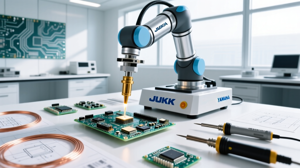
| Laser Soldering | Variable (Localized) | Low (Sequential) | $150,000 - $300,000+ | Heat-sensitive components, micro-BGA, and advanced medical/aerospace devices. |
Thermal Profiling: The Heartbeat of Reflow Soldering
In surface mount assembly, the reflow oven's thermal profile is the most critical variable. The Surface Mount Technology Association (SMTA) emphasizes that a flawed profile is the root cause of over 60% of SMT defects. Modern industrial ovens, such as the Heller 1809EXL or Rehm VisionXP, utilize 8 to 12 distinct heating zones to execute specific profile shapes:
- Ramp-Soak-Spike (RSS): Features a steady ramp (1-2°C/sec), a prolonged soak phase (150°C-190°C) to activate flux volatiles and minimize thermal gradients, and a sharp spike to peak reflow temperature. Ideal for complex boards with mixed component masses.
- Ramp-to-Spike (RTS): A continuous, linear ramp directly to the peak temperature. This profile reduces overall time above liquidus (TAL) and is excellent for preventing tombstoning on small passive components like 0201 and 01005 chip resistors.
Understanding Time Above Liquidus (TAL)
For standard SAC305 (Tin 96.5% / Silver 3.0% / Copper 0.5%) lead-free solder paste, the liquidus temperature is 217°C. Industrial standards dictate that the TAL should be strictly maintained between 45 and 75 seconds. Exceeding 90 seconds risks delaminating the PCB substrate (causing the dreaded 'popcorn effect' in ICs) and degrading the flux, leading to severe oxidation and non-wetting.
Expert Insight: 'When evaluating what soldering means for long-term MTBF (Mean Time Between Failures), the focus must shift from merely achieving a shiny joint to controlling the cooling rate. A controlled cooling rate of 2°C to 4°C per second promotes a fine-grained microstructure in the SAC305 alloy, vastly improving resistance to thermal shock and mechanical drop testing.'
Capital Equipment and Material Costs in 2026
Transitioning from manual soldering to an automated industrial line requires significant capital expenditure. Furthermore, the cost of raw materials has shifted. Due to the volatility in precious metal markets, a 500g jar of high-quality, Type 4 SAC305 solder paste (such as Indium Alloy SAC305 T4) now routinely costs between $160 and $240, depending on the flux chemistry (e.g., ROL0 vs. ROL1).
For a mid-sized contract manufacturer (CM) setting up a baseline SMT line in 2026, the equipment investment typically breaks down as follows:
- Stencil Printer (e.g., MPM Edison): $35,000 - $55,000
- Solder Paste Inspection (SPI): $40,000 - $70,000
- Pick-and-Place Machine (e.g., Yamaha YSM20): $120,000 - $180,000
- Convection Reflow Oven (e.g., BTU Pyramax 75A): $65,000 - $95,000
- Automated Optical Inspection (AOI): $50,000 - $85,000
This $300,000+ baseline ensures the precision required to meet IPC-A-610 Class 3 standards, which are mandatory for automotive, medical, and military applications.
Common Industrial Solder Defects and Failure Modes
Even with premium equipment, process variations can lead to critical defects. Identifying these is crucial for maintaining high MTBF.
1. Head-in-Pillow (HiP)
HiP occurs when the solder paste deposit on the PCB pad and the solder sphere on a BGA (Ball Grid Array) component reflow but fail to fully coalesce, leaving a weak, disconnected boundary. This is often caused by insufficient thermal energy reaching the center of large BGA packages or by excessive oxidation on the BGA spheres. Using a nitrogen-inerted reflow oven (maintaining O2 levels below 500 ppm) drastically reduces HiP occurrences.
2. Tombstoning
Prevalent in ultra-small passives (0402 and smaller), tombstoning happens when one end of a component solders before the other, causing surface tension to pull the component upright. This is mitigated by optimizing pad geometry, ensuring precise stencil aperture reductions, and utilizing an RTS thermal profile to equalize heating across both pads simultaneously.
3. BGA Voiding
Voids are pockets of trapped flux outgassing within the solder joint. While IPC-A-610 allows up to 25% voiding by X-ray area for standard Class 3 assemblies, high-power RF and automotive radar applications often demand voiding below 15% to ensure adequate thermal dissipation. Vacuum reflow ovens are increasingly used in 2026 to pull these gases out of the molten solder before it solidifies.
Conclusion: Soldering as a Science of Reliability
Ultimately, answering the question of what soldering means in an industrial context requires a paradigm shift from viewing it as a simple assembly step to recognizing it as a foundational reliability science. From the precise formulation of no-clean fluxes to the strict thermal management of multi-zone reflow ovens, every variable is engineered to produce a flawless intermetallic bond. For manufacturing engineers and buyers, investing in the right capital equipment, adhering strictly to IPC standards, and continuously monitoring thermal profiles are not just best practices—they are the absolute prerequisites for survival in the modern electronics manufacturing industry.