
The Genesis of Micro Soldering: From Through-Hole to Micro-BGA
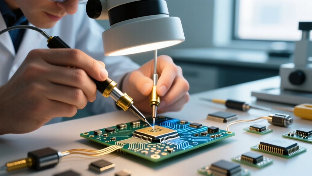
To understand the modern electronics repair landscape, we must first answer a fundamental question: what is micro soldering? At its core, micro soldering is the precise manipulation of solder alloys on surface-mount components (SMDs) measuring less than 1.0mm in length, as well as Ball Grid Array (BGA) integrated circuits with pitch sizes as tight as 0.3mm. Unlike traditional through-hole soldering, which relies on mechanical friction and large thermal masses, micro soldering is an exercise in capillary action, fluid dynamics, and microscopic thermal management.
The discipline was born out of necessity. In the 1980s, the transition from Through-Hole Technology (THT) to Surface Mount Technology (SMT) allowed manufacturers to shrink component footprints. However, the true catalyst for micro soldering was the smartphone revolution of the 2010s. As consumer demand forced Apple, Samsung, and Huawei to pack immense computational power into increasingly thin chassis, engineers began utilizing 0201 and 01005 metric components. By 2026, the bleeding edge of consumer electronics has adopted 008004 (0.3mm x 0.15mm) passives, rendering the unaided human eye entirely obsolete for board-level diagnostics and repair.
Defining the Discipline: The Component Shrinkage Matrix
Micro soldering is not merely 'small soldering.' It is a specialized metallurgical process requiring stereoscopic vision, specialized flux chemistry, and zero-latency thermal delivery systems to prevent substrate damage.
The evolution of component sizes dictates the evolution of the tools required to service them. The following matrix illustrates how the definition of 'micro' has shifted over the decades:
| Era | Component Standard | Dimensions (mm) | Primary Tooling & Technique |
|---|---|---|---|
| 1980s | 1206 | 3.2 x 1.6 | Standard Iron (e.g., Hakko 936), visual inspection |
| 1990s | 0805 / 0603 | 2.0 x 1.25 / 1.6 x 0.8 | Fine-tip iron, basic magnifying lamps |
| 2000s | 0402 | 1.0 x 0.5 | Hot air rework, stereo microscopes, tweezers |
| 2010s | 0201 / Micro-BGA | 0.6 x 0.3 / 0.4mm pitch | Micro-air pencils, tacky flux, BGA stencils |
| 2020s+ | 01005 / 008004 | 0.4 x 0.2 / 0.3 x 0.15 | Nano-cartridge irons, laser soldering, polarized optics |
The Metallurgical and Tooling Evolution
As components shrank, the thermal mass of the solder joints decreased exponentially. This created a paradox: the components became more fragile and susceptible to heat damage, yet the precision required to deliver heat without affecting adjacent components became vastly more complex.
1. Thermal Delivery Systems: The Cartridge Revolution
In the early days of SMT, technicians used ceramic heating elements where the heat had to travel through a metal shaft to the tip. This resulted in severe thermal lag. Today, the undisputed standard for micro soldering is the JBC cartridge system (specifically the C115 and C245 series). In these systems, the heating element and the thermocouple are integrated directly into the very tip of the cartridge. This allows the JBC CD-2BQF station to detect a temperature drop the millisecond the tip touches a copper ground plane, and recover to 350°C in under two seconds. This zero-latency thermal recovery prevents technicians from dwelling on delicate 01005 capacitors, thereby avoiding pad cratering.
2. Optical Enhancements and Polarization
You cannot solder what you cannot see. The evolution of micro soldering is intrinsically tied to the evolution of the trinocular stereo microscope. Modern setups rely on a 7x-45x zoom trinocular head (such as those from AmScope or Swift) mounted on a heavy-duty boom stand. Crucially, a 0.5x Barlow lens is attached to the objective. This doubles the working distance to roughly 15cm, allowing the technician to maneuver a hot air handpiece beneath the lens without melting the glass or obstructing the light path. Furthermore, the introduction of cross-polarizing filters in 2026 has been a game-changer; these filters eliminate the blinding glare that liquid flux typically produces under high-intensity LED ring lights, revealing the actual wetting action of the solder alloy.
3. Flux Chemistry: From Rosin to Synthetic Tack
Flux is the unsung hero of micro soldering. Traditional liquid rosins boil off too quickly and lack the physical viscosity to hold microscopic components in place. The industry has standardized around synthetic, no-clean tacky fluxes, with Amtech NC-559-V2-T3 being a prominent benchmark. This flux serves a dual purpose: its high-tack viscosity acts as a temporary adhesive, holding a 0.4mm 01005 capacitor perfectly in place while the technician applies heat, while its engineered activation temperature ensures that oxides are stripped exactly when the SAC305 (Tin-Silver-Copper) solder reaches its liquidus phase of 217°C.
Real-World Failure Modes in Micro Soldering
According to the IPC-7711/7721 standard for rework and repair, miniaturization introduces specific failure modes that do not exist in macro-soldering. Understanding these is critical for any technician:
- Tombstoning (Drawbridging): Common on 0201 and 01005 components. If one pad heats faster than the other, the surface tension of the molten solder on the hot side will literally stand the component up on its end. Solution: Use a wider hot air nozzle to bathe the entire component in a uniform thermal envelope, or preheat the PCB substrate to 100°C to minimize thermal gradients.
- Pad Cratering: When excessive heat or mechanical force is applied, the copper pad tears away from the FR4 fiberglass substrate, taking a microscopic crater of the laminate with it. This destroys the via connectivity. Solution: Never pull a component while the solder is in a semi-solid (plastic) state. Ensure full liquidus and use precision titanium tweezers.
- Solder Wicking (Capillary Theft): When working near plated through-holes (PTH) or thermal vias, the molten solder will wick down the barrel of the via, leaving the micro-BGA pad dry. Solution: Use a lower-temperature solder alloy (like Sn42/Bi58 which melts at 138°C) for initial rework, or apply via-in-pad plugging techniques prior to component placement.
Architecting Your First Micro Soldering Workbench in 2026
Setting up a professional-grade micro soldering lab requires a strategic allocation of budget. Based on current market pricing, here is a highly actionable, no-compromise equipment list for serious board-level repair:
- Optics ($450 - $600): AmScope 7-45x Trinocular Stereo Zoom Microscope with a 0.5x Barlow lens and a 144-LED dimmable ring light. Do not skimp on the boom stand; a heavy cast-iron base prevents vibration transfer when you bump the desk.
- Soldering Station ($650 - $800): JBC CD-2BQF station paired with the T115-A handle and a selection of C115 cartridges (specifically the 105 and 115 tips for 01005 work, and the 245 handle for larger BGA shields).
- Hot Air Rework ($300 - $400): Quick 861DW. Its brushless motor provides incredibly stable, low-vibration airflow, which is mandatory so you don't accidentally blow 0201 resistors off the board.
- Consumables ($100): Amtech NC-559-V2 tacky flux, Chip Quik SMD291SNL10 (Sn63/Pb37 for easier wetting during repair), and high-precision Dumont #5 titanium tweezers (non-magnetic and anti-solder-wicking).
Guidelines from aerospace bodies, such as those outlined in NASA-STD-8739.3, emphasize that the reliability of a solder joint is entirely dependent on the operator's ability to control the thermal profile and wetting angle. In the micro realm, this control is achieved not through brute force, but through an intimate understanding of metallurgy, fluid dynamics, and optical precision. Whether you are replacing a shorted multilayer ceramic capacitor (MLCC) on a GPU or reballing a 0.35mm pitch NAND flash chip on a smartphone motherboard, mastering the history and physics of micro soldering is the only path to reliable, repeatable repairs.