
Understanding the Types of Soldering Defects Across Assembly Methods
When scaling from prototyping to full-scale PCB manufacturing, or simply upgrading a DIY lab setup, the choice of soldering methodology dictates your yield rate, reliability, and overall cost. While buyers often focus on throughput speeds and equipment pricing, a critical factor in calculating the true cost of ownership (TCO) is understanding the specific types of soldering defects inherent to each process. Wave soldering, reflow soldering, and manual hand soldering each possess unique thermal profiles and mechanical dynamics, leading to distinct failure modes.
In this comprehensive method comparison, we analyze the defect profiles of these three primary techniques. By cross-referencing industry benchmarks from the IPC standards body and reliability data from NASA's NEPP program, we provide engineers and procurement managers with actionable insights to select the right equipment and mitigate yield loss in 2026 and beyond.
The IPC-A-610 Standard: Classifying Soldering Defects
Before comparing methods, it is essential to understand how defects are classified. The IPC-A-610 standard (currently in its latest revisions) categorizes soldering acceptability into three classes:
- Class 1 (General Electronic Products): Focuses on basic functionality. Minor cosmetic defects are acceptable.
- Class 2 (Dedicated Service Products): Requires continued performance and extended life (e.g., consumer electronics, industrial controls). Interrupted service is undesirable but not life-threatening.
- Class 3 (High-Reliability Products): Zero tolerance for equipment downtime (e.g., aerospace, medical life-support). Solder joints must be near-perfect.
A defect that results in a rejected board in Class 3 might be deemed an acceptable 'process indicator' in Class 1. The equipment you buy must be capable of meeting your target IPC class consistently.
Reflow Soldering Defects: High-Volume SMT Challenges
Reflow soldering is the undisputed king of Surface Mount Technology (SMT) for high-volume production. It involves applying solder paste via stencil, placing components, and passing the board through a multi-zone convection oven. While highly automated, the complex thermal profiling required for lead-free alloys like SAC305 (Tin-Silver-Copper) introduces specific defect risks.
1. Tombstoning (Drawbridging)
Tombstoning occurs when a small SMT component (like a 0402 or 0201 resistor) stands up on one end, resembling a tombstone. Root Cause: Uneven wetting forces. If one pad reaches the solder paste's liquidus temperature before the other, the surface tension of the molten solder on the first pad pulls the component upright. Mitigation: Buyers should look for reflow ovens with precise lateral temperature uniformity (e.g., Heller 1809EXL) and ensure pad geometries are thermally balanced in the CAD footprint.
2. Solder Balling and Splatter
Small spheres of solder form around the main joint, risking short circuits. Root Cause: Aggressive preheat ramp rates causing solvents in the solder paste to boil violently and eject molten metal. Mitigation: Maintain a preheat ramp rate of 1°C to 2°C per second. Modern reflow ovens with advanced closed-loop convection control prevent these micro-explosions.
3. BGA Voiding
Gas pockets trapped inside the solder sphere of a Ball Grid Array component. According to the Surface Mount Technology Association (SMTA), voiding exceeding 25% of the X-ray area can compromise thermal and mechanical reliability. Root Cause: Flux volatiles failing to escape the collapsing solder joint. Mitigation: Utilize vacuum reflow ovens, which pull a vacuum during the liquidus phase to physically extract gases before the solder solidifies.
Wave Soldering Defects: Through-Hole and Mixed-Tech Pitfalls
Wave soldering remains vital for through-hole components and heavy power electronics. The board passes over a standing wave of molten solder (typically maintained at 260°C–270°C for lead-free processes). The physical agitation of the wave creates a completely different defect profile compared to the static heating of reflow.
1. Solder Bridging (Shorts)
The most common and costly wave soldering defect, where solder connects two or more adjacent pads or pins. Root Cause: Improper flux application, incorrect conveyor speed, or inadequate preheating causing the solder to lose fluidity before it detaches from the board. Mitigation: Invest in selective wave soldering machines (like the ERSA VERSAFLOW series) for complex mixed-tech boards. These machines use localized micro-waves and nitrogen inerting to eliminate bridging on dense SMT areas.
2. Icicles and Excess Solder
Sharp, downward-pointing spikes of solder hanging from pads or component leads. Root Cause: The solder temperature is too low, or the board preheat is insufficient, causing the solder to freeze prematurely as it separates from the wave. Mitigation: Ensure the wave pot temperature is strictly calibrated to the alloy's specification (e.g., 265°C for SAC305) and verify that flux activators have fully evaporated before hitting the wave.
3. Blowholes and Pinholes
Small holes or craters in the solder fillet, sometimes exposing the component lead. Root Cause: Moisture trapped in the plated through-hole (PTH) barrel or excessive flux volatiles expanding and bursting through the cooling solder. Mitigation: Implement a rigorous PCB baking protocol prior to assembly and utilize top-side preheaters to ensure the entire barrel reaches thermal equilibrium.
Hand Soldering Defects: The Human Element
Manual soldering is unavoidable for prototyping, rework, and low-volume/high-mix production. However, the reliance on human technique introduces high variability. Upgrading from a basic $30 iron to a precision station is the single most effective way to reduce these defects.
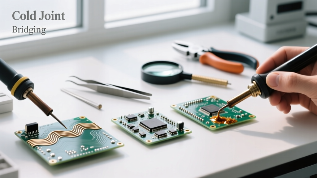
1. Cold Solder Joints
A joint that appears dull, grainy, or lumpy, exhibiting high electrical resistance and mechanical fragility. Root Cause: Insufficient heat transfer to both the pad and the lead simultaneously. Often caused by using a tip with too small a thermal mass for the ground plane being soldered. Mitigation: Use active-tip technology stations like the JBC CD-2BQF or Weller WE1010NA, which detect thermal load and instantly dump wattage into the tip to maintain a stable 350°C interface temperature.
2. Disturbed or Fractured Joints
A joint that crystallizes with a fractured, uneven surface. Root Cause: Movement of the component or wire while the solder is in its 'plastic' (semi-solid) phase between liquidus and solidus temperatures. Mitigation: Implement strict mechanical fixturing and train operators to hold the iron in place for 1-2 seconds after removing the solder wire to allow proper crystallization.
3. Flux Entrapment and Charred Boards
Dark, carbonized residue around the joint or unactivated, sticky flux trapped under components. Root Cause: Dwell times exceeding 3-4 seconds per joint, burning the flux activators and damaging the FR-4 glass transition temperature (Tg). Mitigation: Utilize programmable soldering robots for repetitive manual tasks, or enforce strict dwell-time limits with smart soldering stations that track tip contact time.
Method Comparison Matrix: Defect Probability & Detection
The following matrix compares the three methods based on their most prevalent defect types, typical yield impact, and how easily they are caught by Automated Optical Inspection (AOI).
| Soldering Method | Most Common Defect | Primary Root Cause | AOI Detectability | Typical Yield Impact |
|---|---|---|---|---|
| Reflow (SMT) | Tombstoning | Uneven pad heating / Paste slump | Excellent (Visual) | 1% - 3% loss |
| Wave (THT/Mixed) | Solder Bridging | Poor flux / Wave dynamics | Good (Requires angled lighting) | 2% - 5% loss |
| Hand (Rework/Proto) | Cold Joints | Operator error / Thermal mismatch | Poor (Often requires X-Ray or ICT) | Highly Variable (5%+) |
Equipment Buyer Considerations for Defect Mitigation
When purchasing soldering equipment, the upfront cost is only a fraction of the financial equation. Buyers must evaluate how specific machine features directly target the types of soldering defects outlined above.
- For Reflow Buyers: Prioritize ovens with active cooling zones. Rapid, controlled cooling (3°C to 6°C per second) prevents disturbed joints and refines the grain structure of lead-free alloys, directly improving drop-test reliability.
- For Wave Buyers: Nitrogen (N2) inerting is no longer optional for high-reliability Class 3 boards. N2 environments reduce dross generation by up to 80% and improve solder wetting, virtually eliminating icicles and bridging on fine-pitch connectors.
- For Hand Soldering Buyers: Abandon traditional ceramic heating elements. Invest in inductive or direct-drive resistive heating tips (e.g., Metcal or JBC). These systems respond to thermal demands in milliseconds, preventing the cold joints that plague high-thermal-mass ground planes.
Expert Insight: 'The most expensive defect is the one that escapes your facility. Investing in 3D AOI with multi-spectral lighting for reflow, and flying-probe testing for hand-soldered low-volume batches, will pay for itself within the first quarter by preventing field failures.' — Senior Manufacturing Engineer, Tier 1 EMS Provider.
Frequently Asked Questions (FAQ)
Why does my lead-free hand soldering always look dull compared to tin-lead?
Dullness in SAC305 (lead-free) solder joints is a natural metallurgical characteristic, not necessarily a defect. Lead-free alloys have a different crystalline structure that reflects light poorly. According to IPC-A-610, a dull, matte appearance in lead-free joints is acceptable provided the wetting and fillet contours meet the specified criteria. Do not attempt to 'fix' a dull joint by reheating it, as this will cause copper pad dissolution.
Can selective wave soldering completely replace manual hand soldering?
For mid-to-high volume production, yes. Selective wave machines utilize programmable mini-wave nozzles that can solder complex through-hole connectors placed densely among SMT components without the need for selective solder pallets. While the capital expenditure is high ($80,000 to $150,000+), it eliminates the massive variability and cold-joint risks associated with human operators.
How do I prevent BGA voiding without buying a vacuum reflow oven?
If a vacuum oven is outside your budget, you must optimize your solder paste chemistry. Switch to a paste with a 'low-voiding' flux formulation (often labeled as Type 4 or Type 5 powder with specialized volatile-reduction resins). Additionally, extending the time-above-liquidus (TAL) slightly—while staying under the component manufacturer's maximum thermal limits—gives flux gases more time to escape before the joint freezes.