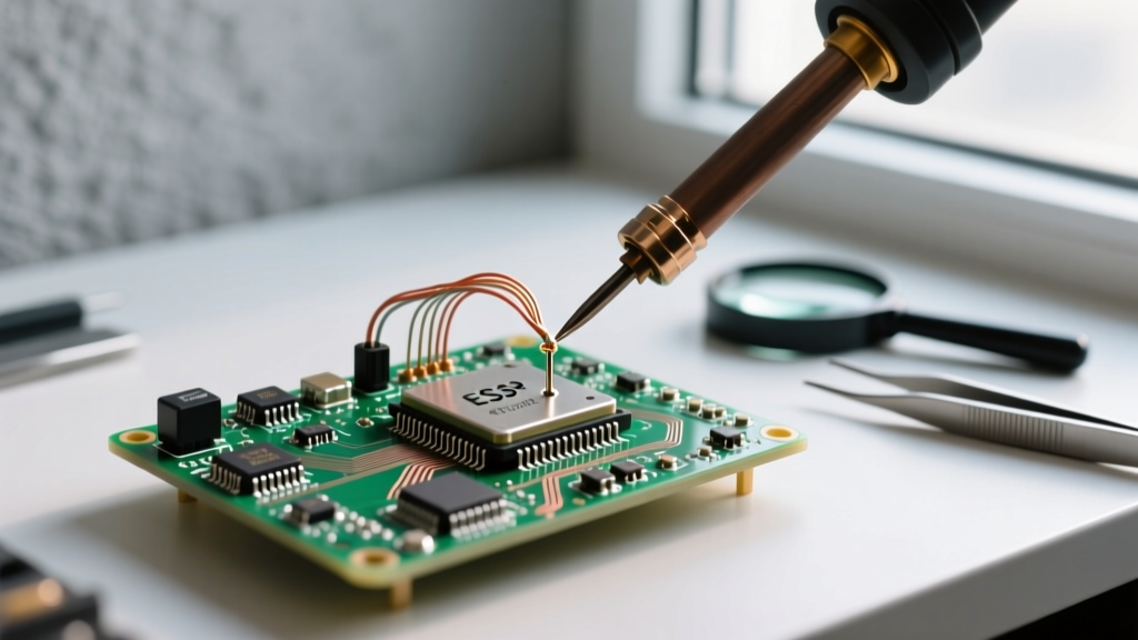

The Physics of Soldering Chips: Why SMD and IC Packages Fail
Soldering chips—ranging from 0.65mm pitch SOICs to ultra-fine 0.4mm TQFPs and bottom-terminated QFNs—requires a fundamental understanding of thermal dynamics, metallurgy, and capillary action. Unlike through-hole components, surface-mount ICs rely entirely on the surface tension of molten solder and the precise activation temperature of chemical fluxes to form reliable intermetallic bonds. When soldering chips in a DIY or low-volume prototyping environment, the margin for error is razor-thin. A variance of just 15°C or a microgram of oxidized flux can result in catastrophic assembly failures.
This comprehensive troubleshooting guide and FAQ addresses the most persistent failure modes encountered when soldering microcontrollers, logic gates, and power management ICs. We will dissect specific defects, provide exact temperature profiles for modern alloys, and outline the precise tooling required to achieve IPC-A-610 Class 2 compliance on your workbench.
Troubleshooting Matrix: Diagnosing Common Chip Soldering Defects
Before reaching for the desoldering wick, you must accurately identify the failure mode. The following matrix details the visual symptoms, root causes, and engineered solutions for the most common defects encountered when soldering chips.
| Defect | Visual Symptom | Root Cause | Corrective Action |
|---|---|---|---|
| Bridging (Solder Shorts) | Solder connects two or more adjacent fine-pitch pins. | Insufficient flux activation, oxidized tip, or excessive solder volume on 0.5mm pitch ICs. | Apply additional no-clean tacky flux. Use a clean, tinned hoof tip (e.g., Hakko T12-K) to drag across the pins, allowing surface tension to pull the bridge away. |
| Tombstoning | Passive component adjacent to the IC stands vertically on one end. | Uneven thermal mass between pads, or the soldering iron heated one pad significantly faster than the other. | Preheat the PCB to 100°C before applying the iron. Ensure pad geometries are symmetrical and solder paste volumes are identical. |
| Cold Solder Joint | Solder appears dull, grainy, or forms a convex bulb rather than a concave fillet. | Insufficient heat transfer to the pad/pin interface, or the chip was moved before the alloy fully solidified. | Reflow the joint with fresh Sn63/Pb37 solder and liquid rosin flux. Hold the iron on the pad for 2-3 seconds to ensure the copper reaches the liquidus temperature. |
| Solder Starvation (ePAD) | QFN or DFN chip shifts laterally; thermal pad lacks sufficient solder connection. | Untented thermal vias wicked molten solder to the bottom layer of the PCB during reflow. | Always tent vias with solder mask or use epoxy-filled/capped vias per IPC guidelines for bottom-terminated components. |
| Lifted Pads | Copper pad delaminates from the FR4 substrate. | Prolonged heat exposure exceeding 5 seconds per pin, or mechanical scraping with a desoldering tool. | Limit iron contact to 3 seconds max. Use low-temperature desoldering braid (e.g., Chemtronics 80-1-5) to minimize thermal soak time. |
Critical FAQs for Microcontroller and IC Assembly
What is the optimal temperature profile for 0.5mm pitch TQFP chips?
The ideal temperature depends entirely on your solder alloy. For traditional Sn63/Pb37 (Leaded) solder, which has a eutectic melting point of 183°C, your soldering station (such as a Weller WT1010 or Hakko FX-951) should be set between 315°C and 330°C. This provides enough thermal headroom to melt the alloy rapidly without lingering on the pad.
If you are working with SAC305 (Lead-Free), which melts between 217°C and 221°C, you must increase your station temperature to 350°C–380°C. Lead-free alloys have a higher surface tension and do not wet copper pads as easily. When soldering chips with SAC305, using a highly active rosin-based flux (RA or RMA) is non-negotiable to break down the rapid oxidation that occurs at these higher temperatures.
How do I prevent voiding and lifting on QFN Thermal Pads?
Quad Flat No-lead (QFN) packages feature an exposed thermal pad (ePAD) on the bottom. A frequent failure mode when soldering chips of this type is 'outgassing.' If your PCB design includes thermal vias directly under the ePAD to transfer heat to inner copper layers, the flux solvents will boil during reflow. The expanding gas travels up through the via, creating massive voids in the solder joint or physically lifting the chip off the board.
Pro-Tip from the Bench: If you are designing the PCB, use via-in-pad with epoxy fill and copper plating (capped vias). If you are working with an existing board that has open vias, use a hot air rework station rather than a soldering iron, and apply a heavy, high-viscosity tacky flux to suppress the outgassing bubbles while the solder is in its liquid phase.
Do I need a hot air rework station for soldering chips?
For prototyping and repairing boards with QFP, SOIC, or SOP packages, a high-quality soldering iron with a micro-hoof tip is often superior and safer than hot air, as it prevents accidental melting of nearby plastic connectors. However, hot air is mandatory for:
- QFN and DFN packages: Where the pins are hidden beneath the chip body and inaccessible to an iron.
- BGA (Ball Grid Array): Requires uniform top-down heating to reflow hundreds of microscopic solder spheres simultaneously.
- Multi-layer ground planes: If an IC pin is connected to a massive internal ground plane, a standard 60W iron will experience severe thermal drop-off. A hot air station (set to 360°C with 400 L/min airflow) provides the volumetric heat required to bring the entire thermal mass up to reflow temperature.
How do I safely clean flux residue from fine-pitch ICs?
Leftover rosin flux can become slightly conductive in high-humidity environments, potentially causing leakage currents between 0.4mm pitch pins. To clean the area after soldering chips, do not simply spray isopropyl alcohol (IPA) and wipe with a paper towel; this merely dissolves the flux and redistributes it under the chip body via capillary action.
Instead, use 99.9% anhydrous IPA (such as MG Chemicals 824) or a dedicated PCB cleaner like Electrolube EFC. Flood the IC pins, agitate gently with a clean, anti-static horsehair brush, and immediately absorb the liquid with a lint-free cleanroom wipe or compressed air to blow the dissolved residue away from the component body.
Advanced Drag Soldering Technique for Fine-Pitch ICs
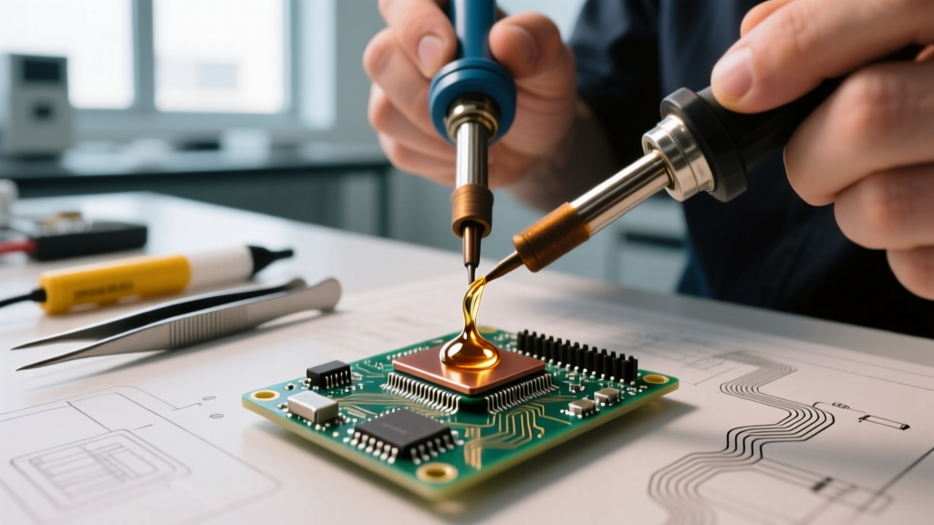
Drag soldering remains the most efficient manual method for soldering chips with 0.5mm and 0.65mm pitch peripheries. Follow this exact sequence to guarantee defect-free joints:
- Preparation: Clean the bare PCB pads with IPA. Apply a microscopic amount of tacky flux (e.g., Chip Quik SMD291AX) to the pads using a syringe with a 0.5mm needle.
- Alignment: Place the IC using precision tweezers. Tack down two diagonally opposite corner pins using a micro-pencil tip to lock the chip in perfect alignment.
- Flux Loading: Apply a generous bead of liquid or tacky flux over the entire row of pins. The flux is the actual 'tool' that prevents bridging.
- The Drag: Load a 2mm hoof tip (K-tip) with a small blob of fresh solder. Hold the iron at a 45-degree angle. Touch the flat of the hoof to the very tips of the pins and slowly drag across the row. Let the flux break the surface tension, pulling the exact right amount of solder into each joint.
- Inspection & Touch-up: Inspect under a 10x magnification loupe or digital microscope. If a bridge remains, add more flux (not more heat) and drag a clean, dry tip through the bridge to wick it away.
Essential Materials and Tooling Specifications
To consistently succeed in soldering chips, your bench must be equipped with materials that match the thermal demands of modern ICs. Below are the recommended specifications for a professional-grade DIY setup:
- Soldering Station: Minimum 65W power output with active tip sensing (e.g., Hakko FX-951, JBC CD-2BE, or Pinecil V2). High thermal recovery is critical when pins are tied to ground planes.
- Flux: No-Clean Tacky Flux. Chip Quik SMD291AX or Amtech NC-559-V2-TF are industry standards for SMD rework.
- Solder Wire: 0.3mm to 0.5mm diameter. Thicker wire introduces too much volume too quickly for fine-pitch ICs. Sn63/Pb37 is highly recommended for manual prototyping due to its superior wetting characteristics.
- Desoldering Braid: 1.5mm width, copper woven with rosin flux core. Avoid using 2.5mm+ braid on fine-pitch chips, as the excessive thermal mass will lift pads.
For further reading on advanced surface mount techniques and industry workmanship standards, consult the Adafruit Guide to Excellent Soldering and review the packaging and reflow guidelines provided by Texas Instruments for specific IC families.