
The Intersection of Optical Physics and Solder Metallurgy
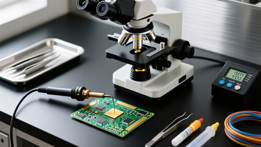
When inspecting modern surface-mount technology (SMT) or reworking ball grid arrays (BGAs), magnification is only half the battle. The true differentiator in high-reliability electronics assembly is material compatibility. Choosing the right stereo microscope for soldering requires a deep understanding of how optical systems interact with specific PCB surface finishes, solder alloy reflectivity, and the chemical byproducts of flux. According to the Association Connecting Electronics Industries (IPC), specifically the IPC-A-610 standard, proper illumination and magnification (typically 10x to 30x) are mandatory for Class 3 high-reliability solder joint inspection. However, the standard assumes an ideal optical setup; in reality, mismatched optics and highly reflective materials like Electroless Nickel Immersion Gold (ENIG) can hide critical defects like micro-cracking or cold solder joints.
In 2026, as component sizes shrink to 01005 and micro-BGA pitches drop below 0.3mm, the material compatibility of your microscope’s lighting, working distance, and lens coatings dictates your success rate. This guide breaks down how to match your stereo microscope configuration to the exact materials and thermal environments of your workbench.
Material Compatibility Matrix: PCB Finishes and Lighting
Different PCB surface finishes interact with light in drastically different ways. A lighting setup that perfectly illuminates a matte Hot Air Solder Leveling (HASL) board will create blinding specular highlights on an ENIG board, masking insufficient wetting or tombstoning defects.
| PCB Surface Finish | Optical Reflectivity | Ideal Lighting Configuration | Defect Masking Risks |
|---|---|---|---|
| ENIG (Gold) | High (Specular) | Polarized Ring Light or Diffused Dome | Glare hiding micro-voids in BGA spheres |
| HASL (Matte Silver/Grey) | Low (Diffuse) | Dual Gooseneck LED (Oblique Angle) | Shadows obscuring cold solder fillets |
| Immersion Silver | Medium-High | Ring Light with Adjustable Polarizer | Surface oxidation mistaken for poor wetting |
| OSP (Organic) | Low (Copper tone) | Warm White (3000K) Dual Arm | Color distortion hiding flux residue burns |
Managing Specular Reflection with Cross-Polarization
When soldering on ENIG or hard-gold edge connectors, standard LED ring lights create a harsh glare that flattens the 3D topography of the solder fillet. To resolve this, professional setups utilize cross-polarization. By placing a polarizing film over the light source and an orthogonal polarizing filter on the microscope objective, you eliminate direct specular reflection. This allows the camera or eyepiece to capture only the scattered light from the actual solder meniscus, revealing the true wetting angle required by NASA Electronic Parts and Packaging (NEPP) high-reliability workmanship standards.
Thermal Plumes, Flux Outgassing, and Lens Degradation
Material compatibility extends beyond what you are looking at to what is floating between you and the workpiece. Soldering with SAC305 (Tin-Silver-Copper) alloys requires tip temperatures of 350°C to 380°C. This generates significant thermal plumes and vaporizes flux activators.
CRITICAL WARNING: Standard stereo microscopes have a working distance (WD) of roughly 90mm to 100mm. At this range, volatile organic compounds (VOCs) from rosin-based and no-clean fluxes will permanently etch the anti-reflective (AR) coatings on standard objective lenses within 6 to 12 months of daily use. Furthermore, sustained thermal plumes can delaminate the cemented doublets inside cheaper eyepieces.
The Barlow Lens Solution for Thermal Protection
To protect your optics from chemical and thermal degradation, you must increase the working distance. Adding a 0.5x auxiliary Barlow lens to a standard 7x-45x zoom stereo microscope achieves two things:
- Increases Working Distance: Pushes the focal plane out to 180mm–200mm, keeping the objective lens safely above the flux outgassing zone and thermal plume.
- Reduces Effective Magnification: Drops the range to 3.5x-22.5x, which is still more than sufficient for 0402 and 0603 SMD inspection while providing a vastly superior depth of field.
For high-volume rework, investing in a specialized objective lens with a chemically resistant, hardened glass coating (often found in industrial-grade Leica or Zeiss optics) is non-negotiable.
2026 Stereo Microscope Configurations for Specific Material Profiles
Based on current market offerings and material-specific requirements, here are the top configurations for different soldering environments.
1. The Hobbyist & General SMD Setup: AmScope SE400-Z
Price Range: $350 – $450
Best For: HASL boards, through-hole, and standard 0805/0603 SMD components using water-soluble fluxes.
Material Compatibility Notes: The AmScope SE400-Z features a robust Greenough optical system that provides excellent 3D depth perception, crucial for judging solder fillet height on matte HASL finishes. However, its standard AR coatings are vulnerable to aggressive rosin flux vapors. Required Upgrade: Pair with a 0.5x Barlow lens immediately to protect the primary objective from flux spatter.
2. The Advanced Rework & ENIG Specialist: Swift SW380T with Polarizer
Price Range: $550 – $700
Best For: ENIG and Immersion Silver PCBs, BGA rework, and 0402 components.
Material Compatibility Notes: The trinocular head allows for the integration of a polarizing filter slider. When combined with a polarized LED ring light, this setup eliminates the blinding glare of gold finishes, allowing for precise inspection of BGA sphere collapse and wetting angles. The SW380T’s CMO (Common Main Objective) design provides a slightly flatter field of view than Greenough, which is preferable when documenting flat BGA pads for IPC compliance reports.
3. The High-Reliability Aerospace Lab: Leica A60 F
Price Range: $1,400 – $1,800+
Best For: Aerospace, medical devices, flex circuits (polyimide), and Class 3 IPC inspection.
Material Compatibility Notes: As detailed in the Leica Microsystems Science Lab, the A60 F utilizes advanced, chemically hardened optics that resist the corrosive nature of halogenated flux activators. Its ergonomic design and superior color rendering index (CRI) lighting allow technicians to distinguish between the subtle amber hue of cured no-clean flux and the dark, carbonized residue of a thermally damaged polyimide flex substrate.
Troubleshooting Material-Specific Optical Anomalies
Issue: Solder Joints Look 'Grainy' or 'Dull' Under the Microscope
Diagnosis: This is rarely a solder defect; it is usually an optical mismatch. If you are using a high-color-temperature (6000K+ cool white) LED ring light on a lead-free SAC305 joint, the natural matte-grey finish of the lead-free alloy will appear artificially grainy and dull, mimicking a cold solder joint.
Solution: Switch to a 4000K-4500K neutral white LED array. This spectrum accurately renders the natural luster of lead-free alloys, allowing you to properly differentiate between a smooth, reflowed meniscus and a disturbed, grainy cold joint.
Issue: Inability to Focus on Both the PCB Trace and the Component Lead Simultaneously
Diagnosis: Depth of field (DoF) collapse. At 45x magnification, the DoF of a standard stereo microscope is less than 0.5mm. If you are inspecting a tall component like a QFP or a cylindrical MELF diode, the top of the component and the solder pad cannot be in focus at the same time.
Solution: Stop down your magnification to 15x-20x. If higher magnification is strictly required, utilize a microscope with an adjustable aperture diaphragm (available on higher-end CMO models) to artificially increase the depth of field, albeit at the cost of slight diffraction.
Frequently Asked Questions
Q: Can I use a digital-only USB microscope instead of a stereo optical microscope for soldering?
A: Digital USB microscopes suffer from severe latency (40ms-100ms) and lack true stereoscopic (binocular) depth perception. While they are adequate for post-soldering documentation, the lack of 3D depth and focal lag makes them dangerous for active soldering, increasing the risk of bridging adjacent pads or lifting thermally sensitive PCB traces.
Q: How often should I clean my objective lens if I use no-clean flux?
A: Even though no-clean flux leaves minimal visible residue, its vaporized activators form a microscopic, oily film on the objective lens that degrades contrast and light transmission. You should gently wipe the outermost surface of your Barlow or objective lens with a microfiber cloth and optical-grade isopropyl alcohol (99%+) every 40 hours of active soldering time.
Q: Does the material of the microscope stand matter for ESD safety?
A: Absolutely. When handling bare, unpopulated PCBs or sensitive MOSFETs, your microscope stand must be ESD-safe. Standard painted cast-iron stands can generate and hold static charges. Ensure your stand, stage plate, and focus rack are constructed from ESD-dissipative materials with a verified path to a common earth ground, maintaining a resistance of 10^6 to 10^9 ohms as per ANSI/ESD S20.20 standards.