
Navigating Soldering Alloys: Beyond the Basics
Selecting the correct solder wire or paste is only the first step in achieving reliable electronic assemblies. As of 2026, the transition to complex lead-free and low-temperature alloys has introduced new failure modes that were virtually non-existent during the era of standard leaded solder. Whether you are hand-soldering a high-density QFN package or reworking a multi-layer motherboard, understanding the metallurgical behavior of your chosen alloy is critical.
This guide serves as a comprehensive FAQ and troubleshooting matrix for the most common soldering alloys used in modern electronics, addressing real-world wetting failures, intermetallic compound (IMC) anomalies, and thermal fatigue.
The 2026 Soldering Alloys Matrix
Before troubleshooting, you must understand the baseline thermal and mechanical properties of your alloy. The table below outlines the primary alloys in use today, including current market pricing and tensile strength metrics.
| Alloy Designation | Composition | Melting Point | Tensile Strength | Avg. Cost (per lb) | Primary Application |
|---|---|---|---|---|---|
| Sn63/Pb37 | 63% Tin, 37% Lead | 183°C (Eutectic) | 52 MPa | $28 - $35 | Prototyping, Aerospace (exempt) |
| SAC305 | 96.5% Sn, 3.0% Ag, 0.5% Cu | 217°C - 220°C | 43 MPa | $45 - $55 | Commercial, Automotive, Consumer |
| Sn42/Bi58 | 42% Tin, 58% Bismuth | 138°C (Eutectic) | 58 MPa | $60 - $70 | Low-temp, LED, Heat-sensitive |
| Sn96.5/Ag3.5 | 96.5% Tin, 3.5% Silver | 221°C (Eutectic) | 41 MPa | $55 - $65 | High-reliability, High-temp |
Troubleshooting FAQ: Flow, Wetting, and Cracking
1. Why is my SAC305 solder beading up and refusing to flow on ground planes?
The Problem: You are using a standard 70W iron (like the Weller WE1010) and SAC305 wire. When touching a large copper pour or ground plane, the solder forms a dull ball and rolls off the pad instead of wetting.
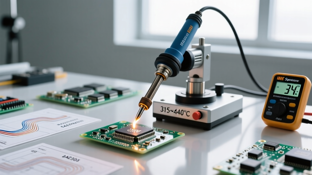
The Root Cause: SAC305 requires significantly more thermal energy to initiate wetting than Sn63/Pb37. The melting point is 217°C, but the working temperature for proper flux activation and wetting is typically 330°C to 350°C. A 70W iron suffers from severe thermal droop when connected to a high-thermal-mass ground plane, dropping the tip temperature below the flux activation threshold (usually 250°C for ROL0 no-clean fluxes).
The Solution:
- Upgrade your thermal delivery: Switch to a direct-cartridge heating system like the JBC CD-2BE with a C245 series tip. These systems detect thermal drain and pump 130W directly into the tip in milliseconds, maintaining the 350°C setpoint.
- Use high-activity flux: If you cannot change irons, apply an external ROL1 (Rosin, Low-activity, halide-containing) liquid flux, such as Kester 951, directly to the pad. The halides will aggressively strip the heavy oxides that form on SAC305 at lower temperatures.
- Pre-heat the board: Use a PCB preheater set to 100°C to reduce the thermal delta between your iron tip and the board.
2. Why do my Sn42/Bi58 (Bismuth) joints crack under minor mechanical stress?
The Problem: You selected a low-temperature Bismuth alloy to protect a heat-sensitive FPC (Flexible Printed Circuit). After assembly, the joints exhibit micro-fractures or fail completely when the cable is bent.
The Root Cause: Bismuth alloys are inherently brittle due to the crystalline structure of Bismuth, which lacks the ductility of lead or pure tin. Furthermore, if the PCB surface finish is HASL (Hot Air Solder Leveling) and contains any trace amount of lead, or if you are soldering to a tinned copper wire with lead, the lead will contaminate the Sn/Bi matrix.
The Metallurgical Failure: The introduction of lead into a Tin/Bismuth system creates a ternary Sn-Pb-Bi eutectic phase that melts at a dangerously low 96°C. Even if the joint doesn't melt, the presence of lead severely embrittles the Bismuth lattice, reducing the fatigue life of the joint by over 80%.
The Solution:
- Never use Bismuth alloys on boards or components that have lead-based finishes. Use ENIG (Electroless Nickel Immersion Gold) or OSP (Organic Solderability Preservative) finishes exclusively.
- For flexible circuits, avoid Sn42/Bi58 entirely. Instead, use a low-silver SAC alloy (like SAC0307) doped with trace Bismuth and Nickel (e.g., SN100C), which maintains ductility while lowering the melting point to ~217°C.
3. What happens if I accidentally mix leaded (Sn63) and lead-free (SAC305) soldering alloys?
The Problem: During a rework session, you used a lead-free solder pot or iron tip previously contaminated with Sn63/Pb37 to rework a RoHS-compliant SAC305 board.
The Root Cause: Mixing these alloys violates IPC-A-610 Class 3 reliability standards for high-performance electronic products. The resulting quaternary Sn-Pb-Ag-Cu system forms complex intermetallic compounds.
The Metallurgical Failure: While lead lowers the melting point (creating pockets that melt around 178°C), the primary danger is the formation of massive, needle-like Ag3Sn (Silver-Tin) intermetallic platelets. These platelets act as stress concentrators within the solder joint. Under thermal cycling (e.g., a device heating up and cooling down during normal use), micro-cracks will initiate at the edges of these Ag3Sn needles and propagate through the joint, leading to catastrophic open-circuit failures months after deployment.
The Solution: Dedicate separate, color-coded soldering stations for leaded and lead-free processes. If contamination occurs on a prototype, use a high-quality solder wick (like Chemtronics 4000 series) with aggressive RA (Rosin Activated) flux to completely scavenge the mixed alloy, clean with 99% IPA, and re-solder with pure SAC305.
Advanced Failure Modes: Whiskers and Copper Leaching
Expert Callout: The 1-to-3 Micron RuleA reliable solder joint relies on the formation of a Cu6Sn5 intermetallic compound (IMC) layer at the boundary between the solder and the copper pad. Under SEM (Scanning Electron Microscope) analysis, a healthy IMC layer should be between 1 to 3 microns thick. If your dwell time is too short, the IMC won't form (non-wetting). If your temperature is too high (>380°C) or dwell time exceeds 4 seconds, the IMC layer grows past 5 microns, becoming excessively thick, brittle, and prone to shear failure.
Tin Whisker Growth in High-Tin Alloys
Pure tin and high-tin alloys (like SAC305, which is 96.5% tin) are susceptible to tin whisker growth. These are spontaneous, hair-like crystalline structures that grow from the solder surface over months or years. In high-voltage or high-density RF circuits, these whiskers can bridge adjacent traces, causing short circuits.
Mitigation Strategy: According to NASA Workmanship Standards, the most effective way to prevent tin whiskers is the addition of at least 3% Lead to the alloy. For strictly RoHS-compliant assemblies where lead is banned, you must apply a conformal coating (such as acrylic or urethane) over the assembled PCB to physically contain any whisker growth, or use matte-tin component finishes which exhibit lower internal compressive stresses than bright-tin finishes.
Copper Dissolution (Leaching) in Wave Soldering
When using high-tin lead-free alloys in wave soldering machines operating at 260°C+, the tin actively dissolves the copper from the PCB pads and component leads. This is known as copper leaching. If the pad dissolves completely, the component will detach from the board.
Mitigation Strategy: To combat this, modern metallurgists add trace amounts of Nickel (Ni) to the solder bath (e.g., SN100C, which is Sn99.3/Cu0.7/Ni0.05). The nickel saturates the molten solder, drastically slowing the dissolution rate of the copper pads while also refining the grain structure of the resulting solder joint, making it brighter and more resistant to thermal shock.
Authoritative References & Further Reading
To ensure your assembly processes meet global reliability standards, consult the following foundational resources on solder metallurgy and workmanship:
- IPC Standards: Review the IPC Soldering Standards portal for the latest updates on J-STD-001 (Requirements for Soldered Electrical and Electronic Assemblies) and IPC-A-610 acceptability criteria.
- NASA Workmanship: The NASA Workmanship Training and Certification Program provides free, highly detailed visual guides and PDFs on identifying IMC fractures, dewetting, and cold joints in mission-critical hardware.
- Indium Corporation: Access phase diagrams and metallurgical whitepapers on advanced alloys via the Indium Solder Alloys Resource Center, an industry leader in specialized electronic assembly materials.