
Decoding the Soldered RAM Meaning in Modern Electronics
When consumers and hardware technicians search for the soldered RAM meaning, they are usually confronting the strict upgrade limitations of modern ultrabooks, gaming handhelds, and Apple Silicon Macs. In semiconductor engineering, 'soldered RAM' refers to Low Power Double Data Rate (LPDDR) memory chips that are packaged in a Ball Grid Array (BGA) format and directly reflowed onto the motherboard's printed circuit board (PCB). Unlike traditional DDR memory, which relies on mechanical SO-DIMM or DIMM slots, soldered RAM eliminates the physical connector entirely.
As of 2026, with the widespread adoption of LPDDR5X and the emergence of LPDDR6 standards operating at speeds exceeding 8533 MT/s, the industry's shift toward soldered memory is no longer just a space-saving tactic—it is an absolute electrical engineering necessity. However, this architectural shift has profound implications for device longevity, repairability, and the advanced microsoldering techniques required to salvage dead boards.
The Engineering Rationale: Signal Integrity and Power Delivery
To understand why manufacturers abandon socketed memory, we must look at high-frequency signal integrity. Modern memory controllers communicate with RAM modules over parallel buses at multi-gigahertz frequencies. At these speeds, the physical distance and the materials the signal travels through dictate performance.
- Trace Length and Impedance: Socketed RAM introduces mechanical pins and connector stubs. These stubs act as antennas, causing signal reflection and degradation (known as insertion loss). Soldering the BGA chip directly to the PCB allows engineers to route ultra-short, tightly controlled impedance traces directly from the CPU to the memory die.
- Power Efficiency: LPDDR architectures are designed for mobile and thin-and-light form factors. By eliminating the mechanical socket and the extra PCB layers required for a DIMM slot, manufacturers reduce parasitic capacitance, lowering the overall power draw of the memory subsystem.
- Z-Height Constraints: A standard SO-DIMM slot adds roughly 3mm to 5mm of vertical Z-height. In devices like the Dell XPS 13 or MacBook Air, where the entire chassis thickness hovers around 11mm, sacrificing 4mm to a plastic RAM slot is physically impossible.
Soldered vs. Socketed RAM: A Technical Comparison
Below is a technical matrix comparing modern BGA soldered memory against traditional socketed alternatives across critical engineering and consumer metrics.
| Feature | BGA Soldered (LPDDR5X) | Socketed (SO-DIMM DDR5) |
|---|---|---|
| Peak Bandwidth (2026) | Up to 8533 MT/s | Up to 6400 MT/s |
| Signal Integrity | Superior (Direct PCB trace routing) | Degraded (Connector stubs & reflections) |
| Power Consumption | Ultra-low (Optimized for mobile/battery) | Moderate to High (Desktop/Workstation) |
| User Upgradability | None (Requires BGA rework station) | High (Plug-and-play module swapping) |
| Failure Point | Solder joint fatigue / Pad cratering | Oxidized gold fingers / Loose slot retention |
The Repairability Crisis and Common Failure Modes
The iFixit Right to Repair advocacy has long highlighted soldered RAM as a primary antagonist to consumer repair rights. When a single memory die fails on a soldered board, the entire motherboard is often deemed 'dead' by authorized service centers, resulting in $800 to $1,500 replacement quotes for a $15 silicon chip.
However, soldered RAM does experience specific physical failure modes that independent microsoldering experts can target:
- Thermal Cycling Fatigue: The coefficient of thermal expansion (CTE) mismatch between the silicon die, the BGA substrate, and the FR4 fiberglass PCB causes microscopic stress on the solder balls during repeated heating and cooling cycles. Over 3 to 5 years, this leads to micro-fractures in the outer rows of the BGA grid.
- Pad Cratering: Mechanical shock (like dropping a laptop) can cause the solder joint to remain intact while tearing the copper pad and underlying resin out of the PCB laminate. This requires intricate trace jumpering under a microscope before a new RAM chip can be installed.
- Underfill Delamination: Manufacturers inject epoxy underfill beneath the BGA chip to reinforce the joints. If the device overheats chronically, the underfill can delaminate, allowing moisture ingress and subsequent electrochemical migration (dendrite growth) between the 0.45mm pitch solder balls.
According to The Repair Association, the deliberate integration of non-upgradable, soldered memory is a leading driver of premature e-waste, forcing consumers to discard otherwise functional logic boards due to single-component failures or insufficient capacity for modern workloads.
Advanced BGA Rework: Can You Replace Soldered RAM?
From a purely physical standpoint, yes—soldered RAM can be desoldered, upgraded, or replaced. However, this is not a DIY task for a standard $30 soldering iron. It requires a professional BGA rework station, precision stencils, and an intimate understanding of thermal profiles. According to JEDEC Solid State Technology Association memory standards, the thermal tolerances for modern memory packaging are strict; exceeding them will delaminate the internal substrate of the RAM chip itself.
Step-by-Step BGA RAM Replacement Workflow
For electronics repair technicians tackling a dead LPDDR5 chip, the rework process follows a strict thermal protocol:
- Step 1: Board Pre-heating. The motherboard is placed on a ceramic pre-heater (e.g., Hakko FR-830) set to 130°C–150°C. This prevents the multi-layer HDI PCB from warping and reduces the thermal shock to surrounding SMD components.
- Step 2: Underfill Softening & Fluxing. A high-tack, no-clean flux like Amtech NC-559-V2-TF is applied to the edges of the chip. The flux capillary action helps transfer heat and prevents oxidation during the melting phase.
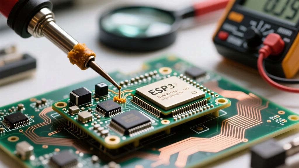
- Step 3: Desoldering. Using a hot air rework station (e.g., Quick 861DW) with a custom 20x20mm nozzle, the technician applies top heat at roughly 320°C. Once the SAC305 lead-free solder balls reach their 217°C melting point, the chip is lifted vertically with vacuum tweezers.
- Step 4: Pad Preparation. The remaining solder on the PCB pads is flattened using high-quality desoldering wick (e.g., Goot Wick CP-3.0-100) and a precision iron set to 280°C. The pads must be perfectly coplanar; any leftover bumps will cause bridging.
- Step 5: Reballing the New IC. The replacement RAM chip is placed in a BGA stencil jig. 0.45mm or 0.5mm SAC305 solder spheres are brushed over the stencil, and a heat gun is used to melt them into perfect spheres on the chip's pads.
- Step 6: Placement and Reflow. The reballed chip is aligned using a microscope and placed onto the flux-tacked PCB pads. The board is returned to the pre-heater, and top heat is applied until the surface tension of the molten solder pulls the chip into perfect alignment (the 'self-centering' effect).
The Firmware Barrier: Software Locks and Provisioning
While the physical soldering process is complex, the software barrier is often the true roadblock. In 2026, simply soldering a larger capacity RAM chip onto a board does not guarantee the system will boot.
Manufacturers like Apple (with their M-series unified memory architecture) and enterprise laptop vendors utilizing Intel Boot Guard or AMD Platform Security Processor (PSP) cryptographically bind the hardware configuration to the motherboard's secure enclave. If you physically replace two 8GB LPDDR5X chips with two 16GB chips, the memory controller may refuse to train the memory, or the system will halt at POST with a firmware mismatch error. Overcoming this requires specialized hardware programmers to read, modify, and reflash the BIOS/ME (Management Engine) region or SPD (Serial Presence Detect) hubs to accept the new memory topology—a reality that keeps advanced board repair highly specialized.
Frequently Asked Questions
Does soldered RAM perform better than socketed RAM?
Yes, in terms of latency and maximum frequency. Because the electrical traces are shorter and lack the interference of a mechanical connector, soldered LPDDR5X can achieve higher bandwidths and tighter timing sub-latencies than equivalent SO-DIMM modules.
Can I upgrade my 8GB soldered laptop to 16GB?
Physically, a microsoldering expert can desolder the existing chips and install higher-density dies, provided there is physical clearance on the PCB and the correct BGA pitch. However, BIOS whitelists and firmware locks often prevent the system from recognizing the new capacity, making it economically unviable for most consumers.
What happens if one soldered RAM chip fails?
If a single BGA memory chip develops an internal short or suffers pad cratering, the system will typically exhibit a 'black screen of death,' fail to pass POST, or show a blinking diagnostic LED code. A board-level repair technician can use thermal imaging and multimeter resistance checks to isolate the faulty chip, desolder it, and replace it to restore the board to full functionality.
Conclusion
Understanding the soldered RAM meaning requires looking past the consumer frustration of non-upgradable laptops and appreciating the extreme high-frequency engineering that makes modern thin-and-light devices possible. While BGA soldering ensures unparalleled signal integrity and power efficiency, it shifts the burden of repair from simple module swapping to advanced microsoldering and firmware manipulation. As memory speeds continue to climb toward the LPDDR6 era, the marriage between silicon and PCB will only grow more permanent, making independent board-level repair skills more vital than ever.