
The reliability of any electronic assembly hinges on the integrity of its solder joints. Before a component ever reaches a printed circuit board (PCB), its ability to form a robust metallurgical bond must be verified. The solderability test method has undergone a radical transformation over the last seven decades, evolving from subjective visual inspections to highly quantitative, AI-assisted metrology. For electronics manufacturers, buyers, and quality assurance engineers in 2026, understanding this evolution is not just an academic exercise—it is critical for selecting the right testing equipment, ensuring compliance with modern IPC standards, and preventing catastrophic field failures.
The Genesis of Reliability: Why Solderability Testing Began
In the early days of consumer electronics and military avionics during the 1950s, soldering was largely an artisanal process. Engineers quickly realized that components stored in warehouses for extended periods developed oxidized terminations. When these oxidized leads were subjected to wave or hand soldering, the molten solder would 'ball up' and reject the surface, leading to cold solder joints and open circuits. The need for a standardized solderability test method became apparent to prevent costly rework and ensure mission-critical reliability in defense applications.
1950s–1970s: The 'Dip and Look' Era and Subjective Metrics
The earliest standardized approach was the Dip and Look method, formalized in early military specifications like MIL-STD-202. The procedure was deceptively simple:
- Preparation: Component leads were dipped in a specific flux (typically Type R or RMA rosin-based).
- Immersion: The leads were submerged in a static solder pot containing molten Tin-Lead (Sn63/Pb37) eutectic alloy at 235°C ±5°C for 2 to 5 seconds.
- Inspection: After cooling, an inspector visually examined the leads under magnification.
The acceptance criterion was generally 95% solder coverage with no pinholes or dewetting. While this method was inexpensive and easy to implement, it suffered from severe limitations. It was entirely subjective, relying on the human eye to estimate coverage percentages. Furthermore, it provided zero data regarding the speed of wetting or the actual mechanical strength of the meniscus force.
1980s–1990s: The Quantitative Leap with Wetting Balance Testing
As surface mount technology (SMT) emerged in the 1980s, component sizes shrank dramatically. The subjective Dip and Look method was no longer sufficient for 0805 or 0603 passive components. The industry required a quantitative solderability test method that could measure the exact physics of wetting.
'The transition from visual estimation to force measurement marked the most significant paradigm shift in solderability testing. We stopped asking if it wetted, and started asking how fast and how strong.' — Historical Archives of the Surface Mount Technology Association (SMTA).
This era birthed the Wetting Balance Test. A wetting balance measures the force exerted on a component lead as it is immersed into a molten solder bath. The resulting force-time curve provides two critical data points:
- Time to Zero Force ($T_0$): The exact moment buoyancy is overcome by the capillary wetting force. A faster $T_0$ indicates superior solderability.
- Maximum Wetting Force ($F_{max}$): The peak upward force exerted by the solder meniscus, indicating the ultimate thermodynamic compatibility of the surfaces.
This quantitative data allowed the IPC Standards committee to develop rigorous, data-driven specifications like IPC J-STD-002 (for component leads) and IPC J-STD-003 (for PCBs), establishing strict millinewton (mN) thresholds and maximum time limits that remain the bedrock of high-reliability testing today.
The 2006 RoHS Shock: Lead-Free Alloys and Thermal Stress
The implementation of the EU RoHS Directive fundamentally disrupted the solderability test method landscape. The ban on lead forced the industry to adopt SAC305 (Sn96.5/Ag3.0/Cu0.5) and other lead-free alloys. This transition introduced massive thermal and metallurgical challenges:
- Higher Processing Temperatures: SAC305 melts at 217°C, requiring test bath temperatures to jump from 235°C to 255°C–260°C.
- Poorer Wetting Characteristics: Lead-free alloys exhibit higher surface tension and slower wetting speeds, causing many legacy components to fail standard $T_0$ thresholds.
- Thermal Degradation: The increased heat exposure during testing risked damaging sensitive plastic IC packages and delaminating PCB substrates.
Testing equipment manufacturers had to redesign solder pots with advanced nitrogen-inerting capabilities to prevent rapid dross formation and oxidation of the lead-free bath, ensuring the test environment accurately simulated modern reflow and wave soldering processes.
2020s and Beyond: Automated Optical Inspection (AOI) and AI
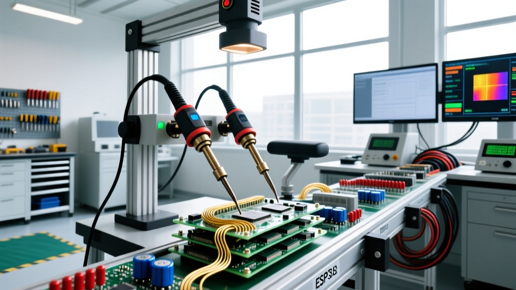
As we navigate 2026, the solderability test method has expanded beyond the metallurgical lab and onto the production floor. Modern manufacturers utilize 3D Automated Optical Inspection (AOI) and X-ray systems to verify solderability outcomes in real-time. Advanced AOI systems now employ machine learning algorithms trained on millions of solder joint profiles to detect micro-dewetting, graping, and head-in-pillow (HiP) defects that human inspectors would miss.
Furthermore, the rise of low-temperature alloys like Tin-Bismuth-Silver (SnBiAg) for energy-efficient manufacturing has prompted new testing protocols. These alloys melt as low as 138°C, requiring highly sensitive wetting balances capable of operating at lower thermal masses while maintaining strict buoyancy corrections.
Comparative Matrix: Evolution of Solderability Test Methods
| Era | Primary Test Method | Key Metric / Output | Relevant Standard | Pros & Cons |
|---|---|---|---|---|
| 1950s–1970s | Dip and Look | Visual % Coverage | MIL-STD-202, Early IPC | Pro: Low cost. Con: Highly subjective, no speed data. |
| 1980s–1990s | Wetting Balance | Force (mN) & Time ($T_0$) | IPC J-STD-002 / 003 | Pro: Quantitative, repeatable. Con: Expensive equipment, slow throughput. |
| 2000s | Globule Test | Time to envelopment | IPC J-STD-002 | Pro: Good for small SMT leads. Con: Difficult to automate, messy. |
| 2020s+ | AI-Driven AOI & 3D X-Ray | Volumetric defect mapping | IPC-A-610 (Post-solder) | Pro: 100% inline inspection. Con: Tests the joint, not the raw component. |
Practical Buyer’s Guide: Selecting a Solderability Test Method Today
If you are outfitting a quality control lab or upgrading a manufacturing facility in 2026, choosing the right solderability test method requires balancing budget, throughput, and compliance requirements. Based on current market offerings from leaders like Rhesca, Microconductive, and Kurtz Ersa, here is a strategic framework:
1. Entry-Level QC & Incoming Inspection (Budget: $3,000 – $8,000)
For small contract manufacturers or hobbyist labs verifying incoming PCB batches, a modernized Dip and Look station equipped with digital microscopy is sufficient. Modern setups replace the human eye with a 4K digital microscope and image analysis software that automatically calculates solder coverage percentage. Actionable Advice: Ensure your solder pot features digital PID temperature control (±2°C accuracy) and an integrated fume extraction system. When testing lead-free boards, always use a nitrogen-shrouded pot to prevent the SAC305 bath from oxidizing during the test sequence.
2. High-Reliability & Aerospace Labs (Budget: $35,000 – $75,000)
For medical, automotive (AEC-Q qualified), and aerospace applications, a Wetting Balance Tester is non-negotiable. Modern systems (such as the Rhesca SAT series) feature automated dipping mechanisms, integrated buoyancy correction algorithms, and nitrogen-inerted solder baths. Actionable Advice: When purchasing a wetting balance, verify that the software natively supports the latest IPC J-STD-002G (or newer) pass/fail criteria. Look for systems that offer 'meniscus scan' capabilities, which map the wetting force across the entire width of a gull-wing lead, identifying localized oxidation issues that a single $F_{max}$ reading might obscure.
3. High-Volume Inline Verification (Budget: $100,000+)
For high-volume SMT lines, raw material testing is supplemented by inline 3D AOI and SPI (Solder Paste Inspection). While SPI verifies paste volume before reflow, 3D AOI verifies the final solderability outcome. According to Indium Corporation Technical Documents, combining advanced flux chemistries with real-time AOI feedback loops reduces field failure rates related to poor solderability by over 85%.
Conclusion
The solderability test method has evolved from a crude visual check into a sophisticated science of thermodynamics and machine vision. Whether you are relying on the quantitative precision of a wetting balance to meet IPC J-STD-002 requirements or deploying AI-driven AOI to catch micro-defects on the assembly line, understanding the historical context and physical limitations of these methods is essential. By selecting the testing paradigm that aligns with your specific alloy profiles and reliability targets, you ensure that every solder joint leaving your facility is built to withstand the demands of modern electronics.