
The Core Dilemma: PoP vs. Discrete Soldered Memory
As edge AI accelerators and ultra-compact mobile SoCs push memory bandwidth requirements past 8533 Mbps with LPDDR5X, the physical interconnect between the processor and RAM has become a primary bottleneck. For hardware engineers and PCB designers in 2026, the architectural choice between Memory on Package (PoP) and Discrete Soldered Memory dictates not just signal integrity, but thermal envelopes, manufacturing yields, and end-of-life repairability.
This decision framework cuts through the marketing jargon to provide a rigorous, data-driven comparison of stacking memory directly onto the SoC versus routing it across a high-density interconnect (HDI) printed circuit board.
Terminology Clarification:
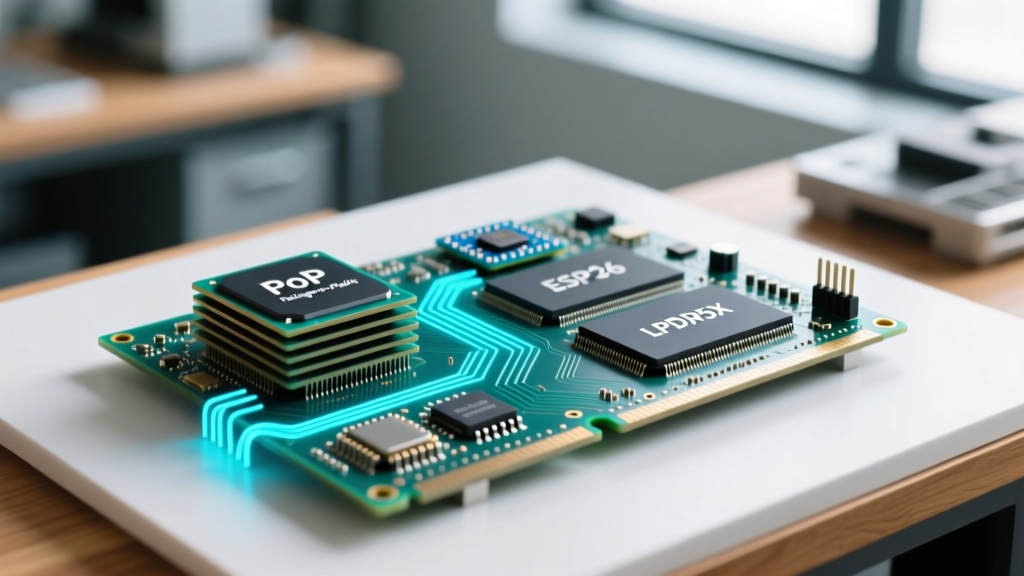
Package-on-Package (PoP): The memory BGA (Ball Grid Array) is soldered directly onto the top land pads of the SoC BGA. The combined stack is then soldered to the main PCB.
Discrete Soldered: The SoC and memory chips are separate components, both soldered independently to the surface of the PCB, requiring complex trace routing between them.
2026 Decision Matrix: Architecture Comparison
Before diving into the physics and economics, review this high-level comparison matrix to align the architecture with your product's primary constraints.
| Design Parameter | Memory on Package (PoP) | Discrete Soldered (PCB-Mounted) |
|---|---|---|
| Form Factor | Ultra-compact (Z-axis stacking) | Larger X-Y footprint required |
| Signal Integrity | Superior (sub-millimeter vias) | Challenging (requires strict length matching) |
| Thermal Profile | Poor (SoC heat bakes RAM) | Excellent (independent heat dissipation) |
| PCB Complexity | Low (4-6 layers typical) | High (8-12 HDI layers required) |
| Reworkability | Near impossible in the field | Feasible with IPC-7711/21 standards |
| NRE & Unit Cost | High assembly cost, low PCB cost | Low assembly cost, high PCB cost |
Deep Dive: Package-on-Package (PoP) Architecture
PoP is the undisputed king of smartphones and ultra-thin tablets. By stacking the LPDDR5X die directly atop the application processor, designers eliminate the need to route high-speed differential pairs across the PCB.
Signal Integrity and the 0.4mm Pitch Challenge
In a PoP configuration, the connection between the SoC and the memory utilizes a microscopic 0.4mm pitch BGA. Because the traces are contained entirely within the package substrate, they are measured in fractions of a millimeter. This virtually eliminates crosstalk, skew, and electromagnetic interference (EMI) that plague PCB traces. According to the JEDEC JESD209-5-1 LPDDR5X standard, maintaining signal integrity at 8533 Mbps requires incredibly tight timing margins that PoP naturally satisfies without complex PCB tuning.
Thermal Bottlenecks and Capillary Underfill
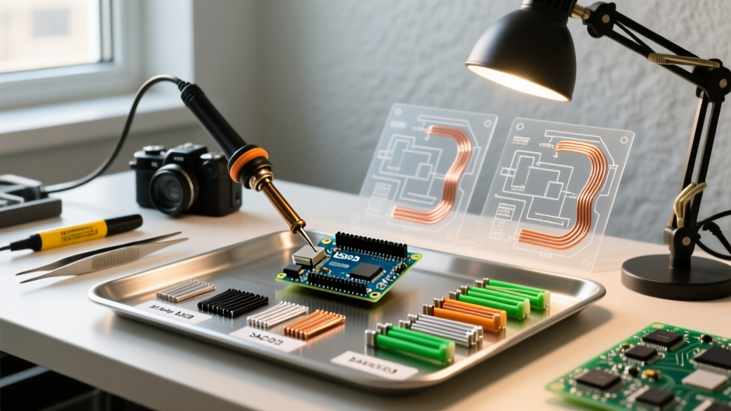
The fatal flaw of PoP is thermodynamics. Modern 4nm and 3nm SoCs can draw upwards of 12W under sustained AI workloads. Because the memory is stacked directly on top of the SoC, the DRAM acts as a thermal insulator, trapping heat. Furthermore, DRAM retention rates degrade significantly as temperatures exceed 85°C. To prevent the stack from delaminating during the 245°C peak reflow temperatures required for SAC305 lead-free solder, manufacturers must inject Capillary Underfill (CUF) between the packages. This CUF adds mechanical strength but further exacerbates the thermal trapping effect, forcing system architects to implement aggressive vapor chamber cooling or graphite heat spreaders.
Deep Dive: Discrete Soldered Memory
Discrete soldered memory remains the standard for single-board computers (SBCs), automotive ADAS modules, and enterprise edge gateways. While it consumes more board space, it offers distinct advantages in thermal management and manufacturability.
PCB Stackup and Impedance Control
Routing LPDDR5 or LPDDR5X from an SoC to a discrete BGA requires an HDI (High-Density Interconnect) PCB. For a 2026 edge AI board, you will typically need a 10-layer to 12-layer stackup with microvias to escape the 0.65mm or 0.8mm pitch BGA pads. The Texas Instruments DDR Routing Guidelines mandate strict 100-ohm differential and 50-ohm single-ended impedance controls. Furthermore, all data strobe (DQS) and clock traces must be length-matched to within 5 mils (0.005 inches) per byte lane. Failure to achieve this precision results in bit errors and boot failures.
Reworkability and IPC Standards
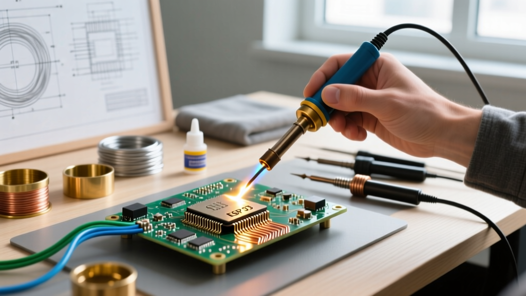
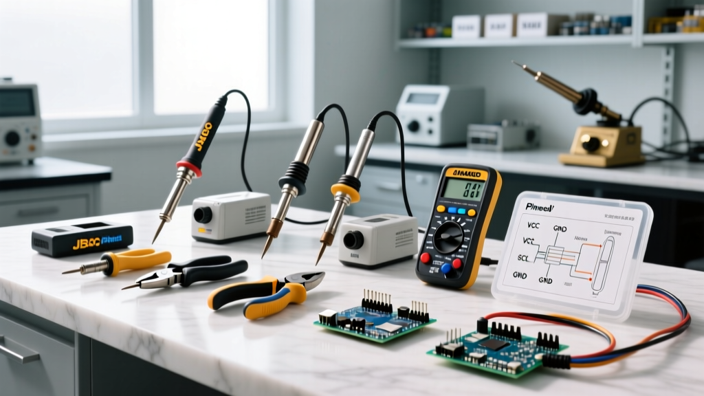
Unlike PoP, discrete memory can be replaced if a chip fails during manufacturing or in the field. Following the IPC-7711/21 Rework Standard, a trained technician using a precision hot-air rework station and a localized nitrogen preheater can safely desolder a defective discrete BGA, clean the pads with flux and desoldering wick, and reball a replacement chip. Attempting this on a PoP stack will almost certainly destroy the underlying SoC due to the coupled thermal mass and fragile 0.4mm interconnects.
Manufacturing & Assembly Cost Analysis
When scaling from prototype to a 50,000-unit production run, the cost dynamics between PoP and discrete soldered memory invert.
- PoP Assembly Costs: Requires specialized SMT (Surface Mount Technology) lines capable of dip-fluxing the top BGA and placing it with sub-20-micron accuracy. X-ray inspection (AXI) is mandatory to verify hidden solder joints. Expect to add $1.50 to $3.00 per unit in specialized assembly and inspection time.
- Discrete PCB Costs: While SMT assembly is standard and cheap, the PCB itself is expensive. A 10-layer HDI board with blind/buried vias and tight impedance tolerances costs $4.00 to $8.00 more per board than a standard 6-layer PoP-compatible board.
- Yield Losses: PoP suffers from 'head-in-pillow' solder defects if the warpage of the SoC and memory packages do not match during reflow. Discrete memory suffers from open/short circuits if HDI microvias fail during the PCB fabrication process.
The 2026 Decision Framework: Step-by-Step
Use this sequential logic flow to finalize your memory architecture choice:
- Evaluate the Z-Axis Constraint: If your enclosure thickness is under 6mm (e.g., wearables, smartphones), PoP is mandatory. If you have 10mm+ of vertical clearance, proceed to step 2.
- Calculate the Thermal Envelope: If the SoC TDP exceeds 8W and active cooling is absent, avoid PoP. The thermal throttling will negate the bandwidth advantages of LPDDR5X. Choose discrete memory to allow independent heatsinking.
- Assess Production Volume: For runs under 5,000 units, the NRE (Non-Recurring Engineering) costs of designing a 12-layer HDI PCB for discrete memory may be unjustifiable. PoP allows you to use a cheaper 6-layer PCB, shifting the complexity to the silicon vendor who provides the pre-tested stack.
- Determine Repairability Requirements: If designing for automotive, aerospace, or high-end industrial IoT where field-replaceable modules or high salvage rates are required, discrete soldered memory is the only viable option.
Expert Verdict
There is no universal 'best' choice between memory on package vs soldered discrete configurations; there is only the right choice for your specific physical and economic constraints. For ultra-dense consumer electronics where every millimeter of X-Y board space commands a premium, PoP remains an engineering marvel despite its thermal penalties. However, for the booming 2026 sector of edge AI, robotics, and industrial SBCs, discrete soldered memory on an HDI stackup provides the thermal headroom, signal debugging access, and reworkability required to ensure long-term product viability.