
Understanding J-STD Soldering Standards
When manufacturing, repairing, or inspecting high-reliability electronics, adhering to J-STD soldering protocols is not optional—it is the baseline for safety and functionality. The term 'J-STD' primarily refers to two foundational documents published by the IPC (Association Connecting Electronics Industries): IPC J-STD-001 (Requirements for Soldered Electrical and Electronic Assemblies) and IPC-A-610 (Acceptability of Electronic Assemblies). While J-STD-001 dictates the materials, processes, and criteria for creating the solder joint, IPC-A-610 provides the visual benchmarks for inspection.
As of 2026, the push toward miniaturization, high-density interconnects (HDI), and the explosive growth of EV (Electric Vehicle) power electronics have made J-STD compliance more critical than ever. A solder joint that passes a basic visual check might still fail electrically or mechanically if the intermetallic compound (IMC) layer was compromised by improper thermal profiles. This guide breaks down the exact requirements, equipment investments, and material specifications needed to achieve true J-STD compliance in your workshop or production floor.
The Three Classes of Electronic Assemblies
IPC J-STD-001 categorizes electronic products into three distinct classes based on their end-use environment and reliability requirements. Understanding which class your project falls into dictates your tooling, inspection magnification, and acceptable defect margins.
| Class | Designation | Typical Applications | PTH Barrel Fill Requirement | Inspection Rigor |
|---|---|---|---|---|
| Class 1 | General Electronic Products | Consumer gadgets, toys, basic lighting | Not strictly mandated / Visual only | Low (Visual 1x-3x) |
| Class 2 | Dedicated Service Products | Industrial controls, telecom, automotive | Minimum 50% | Medium (3x-5x) |
| Class 3 | High-Performance Products | Medical life-support, aerospace, military | Minimum 75% | High (10x-30x) |
For NASA Workmanship Standards and aerospace contractors, Class 3 is the absolute minimum, often supplemented by NASA-STD-8739.3. In Class 3 J-STD soldering, a plated through-hole (PTH) component must exhibit at least 75% barrel fill with proper wetting on both the top and bottom lands, ensuring mechanical strength against extreme vibration and thermal cycling.
Selecting a Soldering Station for J-STD Compliance
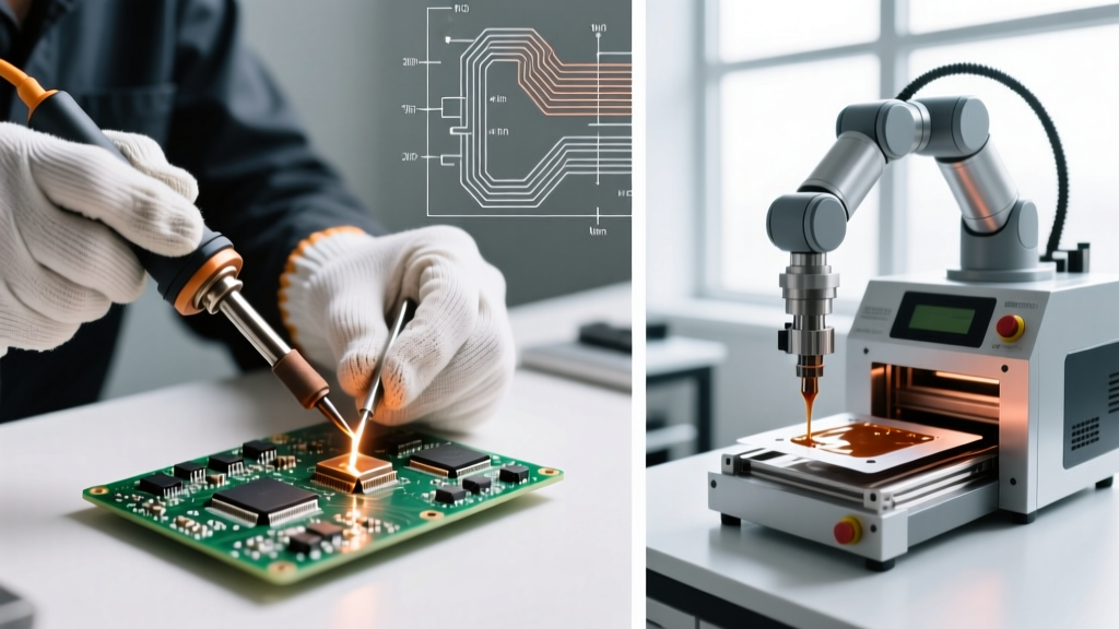
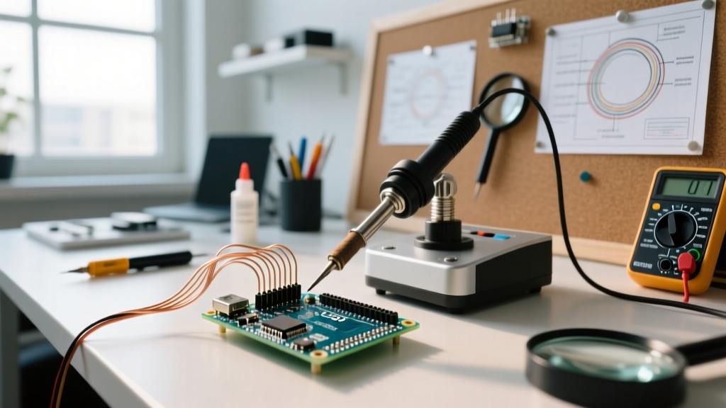
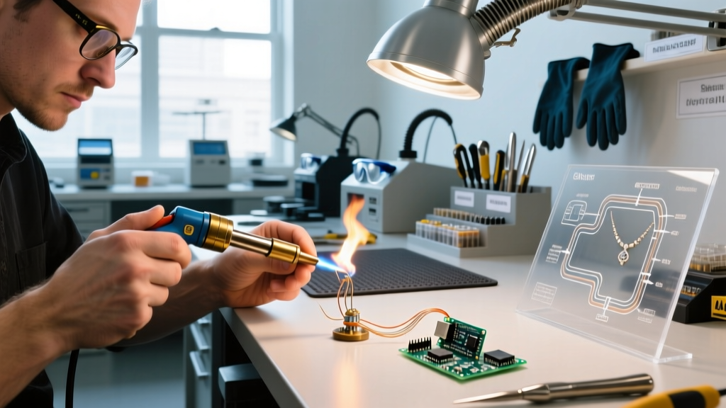
You cannot achieve J-STD-001 compliance with a basic, uncalibrated ceramic heater iron. The standard requires strict control over thermal recovery, dwell time, and ESD (Electrostatic Discharge) safety. When a 4-layer PCB with heavy ground planes acts as a massive heatsink, an underpowered iron will cause the operator to increase dwell time to compensate, leading to pad delamination and excessive IMC growth.
Top-Tier Station Recommendations (2026 Market)
- JBC CD-2BQE (approx. $550): The industry darling for Class 3 rework. JBC's exclusive heating system places the thermocouple directly inside the tip cartridge, achieving 350°C from cold in under 2 seconds. This allows operators to use lower baseline temperatures (e.g., 300°C for SAC305), preserving flux activity and preventing component thermal shock.
- Weller WXP 120 / WE 1010 ($120 - $400): The WE 1010 is an excellent entry-level ESD-safe station for Class 2 work. However, for heavy multilayer boards, the WXP 120 with its 120W power output and Weller's proprietary silver-layer heating elements provide the necessary thermal mass recovery.
- Metcal CV-5200 ($650+): Utilizing SmartHeat inductive technology, Metcal stations automatically adjust power output based on the thermal load of the joint. This is highly favored in aerospace J-STD soldering because it removes operator guesswork, preventing accidental overheating of sensitive RF components.
Tip Geometry and Selection
J-STD compliance requires matching the tip geometry to the pad size. Using a massive chisel tip on a 0402 SMT pad risks bridging and tombstoning, while using a micro-conical tip on a large ground tab will result in a cold solder joint. For standard 0603 to 0805 SMT components, a JBC C245-945 (bent conical) or a Weller RT4 (0.4mm chisel) provides optimal heat transfer. For PTH components, a bevel or 'hoof' tip is recommended to facilitate proper solder flow and capillary action into the barrel.
Consumables: Solder Alloys and Flux Classifications
The materials you introduce to the joint are governed by IPC J-STD-004 (Requirements for Soldering Fluxes) and IPC J-STD-006 (Requirements for Electronic Grade Solder Alloys).
Solder Alloy Selection
While Sn63/Pb37 (Leaded) remains popular for prototyping and specific military exemptions due to its low melting point (183°C) and lack of tin whisker growth, the vast majority of 2026 commercial J-STD soldering utilizes Lead-Free alloys. SAC305 (Sn96.5 / Ag3.0 / Cu0.5) is the benchmark. It melts between 217°C and 220°C. Because of this higher liquidus temperature, SAC305 requires specialized flux chemistries that do not burn off at 320°C tip temperatures.
Flux Chemistry (J-STD-004)
Flux is categorized by composition, activity level, and halide content. For high-reliability Class 3 assemblies where cleaning is difficult or impossible, you must use a ROL0 (Rosin, Low Activity, 0% Halides) or ORL0 (Organic, Low Activity, 0% Halides) flux. These fluxes leave a benign, non-conductive residue that will not cause electrochemical migration (dendritic growth) in humid environments. Avoid high-halide (ROM1/L1) fluxes unless you have an automated aqueous or saponifier cleaning process validated to remove all ionic residues post-solder.
Expert Insight: Never mix flux types. Applying a water-soluble (ORH1) flux over a no-clean (ROL0) residue can activate the dormant no-clean resin, creating a highly corrosive, conductive matrix that will short high-impedance circuits over time.
Common J-STD Defects and Failure Modes
According to the IPC-A-610 Acceptability Guidelines, inspectors must look for specific anomalies that compromise joint integrity. Here are the most common failures encountered during J-STD audits:
- Disturbed Solder Joint: Characterized by a frosty, grainy appearance with visible ridges. This occurs when the component or wire moves while the solder is in its plastic (semi-solid) phase during cooling. It creates micro-fractures in the IMC layer, leading to intermittent open circuits.
- Cold Solder Joint: Caused by insufficient heat transfer. The solder balls up on the lead or pad without wetting the surface, resulting in a high-resistance connection. The wetting angle exceeds 90 degrees, which is an automatic reject in Class 2 and Class 3.
- Solder Wicking (Thieving): Occurs when flux and solder travel too far up a wire strand or component lead, away from the termination point. This stiffens the wire, removing its flexibility and creating a stress concentration point that will snap under vibration.
- Insufficient PTH Barrel Fill: Failing to achieve the 50% (Class 2) or 75% (Class 3) vertical fill inside a plated through-hole. This is often caused by a poorly designed thermal relief on inner layers, which acts as a heatsink, freezing the solder before capillary action can pull it through the barrel.
Inspection and Magnification Requirements
J-STD soldering requires verification beyond the naked eye. The IPC mandates specific magnification levels based on the board's technology and component density. For standard through-hole and larger SMT (1206+), 3x to 5x magnification is sufficient. However, for micro-BGA, QFN, and 0201 passives, inspectors must utilize 10x to 30x stereo microscopes or automated optical inspection (AOI) systems. Proper coaxial lighting is just as critical as magnification; without it, inspectors cannot accurately judge the wetting angle or detect microscopic micro-cracks in the solder fillet.
Certification and Training Costs in 2026
Equipping a shop is only half the battle; human execution is the primary variable in J-STD soldering. To guarantee compliance, facilities invest in CIS (Certified IPC Specialist) training for their operators. As of 2026, a standard 4-day CIS course for IPC J-STD-001 and IPC-A-610 costs between $1,600 and $2,400 per operator, depending on the training center and whether the facility hosts the instructor on-site. While this represents a significant upfront capital expenditure, the ROI is realized through drastically reduced field failure rates, scrap reduction, and the ability to bid on lucrative medical and defense contracts that mandate certified personnel.
Summary Checklist for J-STD Compliance
- Verify your soldering station is ESD-safe and features closed-loop thermal recovery.
- Select the correct solder alloy (SAC305 for lead-free, Sn63 for exempt legacy) and match the flux to J-STD-004 (ROL0 for no-clean high-reliability).
- Define your IPC Class (1, 2, or 3) before starting the build to establish barrel fill and wetting angle targets.
- Use appropriate magnification and lighting for post-solder inspection.
- Maintain annual calibration logs for all soldering equipment and thermocouples.
Mastering J-STD soldering is an ongoing commitment to process control. By investing in precision thermal tools, understanding flux chemistry, and strictly adhering to IPC visual benchmarks, you elevate your electronics from hobbyist assemblies to professional, mission-critical hardware.