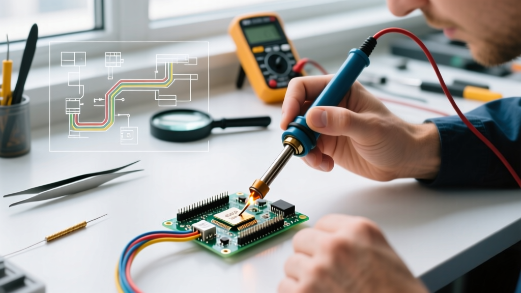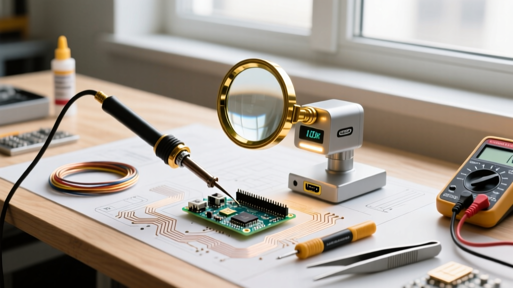

When surface-mount technology (SMT) first transitioned from industrial assembly lines to hobbyist workbenches, the physical scale of components plummeted. Today, hand-soldering 0201 (0.6mm x 0.3mm) or even 01005 (0.4mm x 0.2mm) imperial components is a routine requirement for electronics repair and prototyping. Because the human eye struggles to resolve details smaller than 0.1mm at a comfortable working distance, the humble magnifying glass for soldering has undergone a radical, multi-decade evolution.
Understanding this history is not just an academic exercise; it is the key to making an informed purchasing decision. The market is currently flooded with legacy optical designs, mid-tier stereo microscopes, and ultra-modern digital imaging systems. This guide traces the technological lineage of bench magnification and provides a 2026 buyer’s framework to help you select the exact tool your work demands.
The Early Days: Optical Lenses and the Halo Ring Era (1980s–2000s)
Before the proliferation of micro-controllers and dense SMD layouts, through-hole components dominated electronics. The standard magnifying glass for soldering was the optical halo ring—a heavy, circular fluorescent or incandescent lamp with a built-in glass or Fresnel lens. Brands like Daylight and Panavise popularized these bench staples.
- Magnification: Typically fixed at 2x to 5x.
- Optical Quality: Basic spherical glass or acrylic Fresnel lenses. These suffered heavily from chromatic aberration (color fringing) and edge distortion.
- The Soldering Experience: Users had to hunch over the lens, peering through a narrow "sweet spot" in the center of the glass. Depth perception was entirely monocular, making it incredibly difficult to judge the Z-axis height of a soldering iron tip relative to a delicate component pad.
While a basic 3x/5x flip-lens headset or halo ring (costing between $40 and $80 today) remains adequate for basic through-hole wiring or large terminal crimping, it is fundamentally obsolete for modern SMT rework.
The Binocular Shift: Stereo Microscopes Enter the Bench (2005–2015)
As component density increased, the industry adopted the stereo binocular microscope. Unlike compound biological microscopes that use a single objective lens split into two eyepieces (yielding a flat, 2D image), stereo microscopes utilize a Greenough or Common Main Objective (CMO) optical system. This provides two entirely separate optical paths, delivering true 3D depth perception.
Why 3D Depth Perception Matters in Soldering
When dragging a micro-soldering iron across a QFP (Quad Flat Package) IC, you must maintain a precise 0.5mm clearance to avoid melting adjacent plastic connectors. Stereo vision allows your brain to process spatial depth, making hand-eye coordination intuitive. Models like the AmScope SM-4TZ or OMAX trinocular heads became the gold standard, dropping in price from $2,000+ lab-grade equipment to accessible $350–$500 hobbyist units.
The Digital Disruption: HDMI Screens and the Latency Problem (2016–2023)
The next evolutionary leap was the removal of the eyepieces entirely. Digital microscopes, featuring a camera sensor mounted to a boom arm and outputting to an HDMI monitor, promised an end to the severe neck strain associated with peering down binocular tubes. Early models from brands like Hayear and Andonstar were revolutionary but introduced a critical flaw: latency.
"In micro-soldering, a video feed delay of even 120 milliseconds creates a severe hand-eye disconnect. The operator moves the iron, but the screen updates a fraction of a second later. This lag is the primary cause of bridged pads and scorched PCBs among digital scope adopters."
Furthermore, early digital sensors (often repurposed smartphone webcams) lacked the dynamic range to handle the harsh contrast between a bright, reflective pool of molten solder and the dark, flux-stained FR4 fiberglass of a circuit board.
2026 Buyer’s Matrix: Which Generation Fits Your Bench?
Today, the market has matured. Modern digital sensors have largely solved the latency issue, while optical stereo scopes remain unbeatable for pure depth perception. Use the matrix below to align your budget and technical requirements with the correct generation of magnification.
| Feature | Optical Halo / Headset | Stereo Binocular (e.g., AmScope) | Modern Digital HDMI (e.g., Andonstar AD409 Pro) |
|---|---|---|---|
| Avg. Price (2026) | $40 – $90 | $350 – $600 | $300 – $550 |
| Depth Perception | None (Monocular) | Excellent (True 3D Stereo) | None (2D Flat Screen) |
| Latency | Zero | Zero | < 30ms (Imperceptible) |
| Ergonomics | Poor (Neck/Back Strain) | Moderate (Fixed Tube Angle) | Excellent (Eye-Level Monitor) |
| Best Use Case | Through-hole, wire splicing | Complex BGA rework, 01005 SMD | PCB trace repair, recording, long sessions |
Critical Specifications to Demand
Regardless of whether you choose an optical or digital path, the IPC visual inspection standards dictate that solder joints must be evaluated for wetting, fillet shape, and voiding. To achieve this, your equipment must meet specific hardware benchmarks.
Working Distance (WD) and Auxiliary Lenses
Working distance is the physical space between the bottom of your lens and the PCB. Standard stereo microscopes have a WD of about 90mm. This is often insufficient to fit a soldering iron handpiece and a fume extractor nozzle simultaneously. Actionable Advice: Always purchase a 0.5x auxiliary objective lens (Barlow lens). This screws onto the bottom of a stereo scope, doubling your working distance to ~180mm while halving the magnification (which you can easily compensate for by zooming the eyepieces). For digital scopes, ensure the physical stand allows for at least 150mm of vertical clearance.
Illumination: Defeating Flux Glare
Built-in ring lights are the enemy of solder inspection. They blast light directly down the optical axis, causing severe specular reflection (glare) off molten solder and wet flux, blinding the sensor or your eyes. The professional standard is dual-arm gooseneck LED lighting positioned at 45-degree angles to the workpiece. For digital scopes, look for models featuring hardware-level polarization filters, which cut through flux glare and reveal the actual topology of the solder fillet.
Real-World Failure Modes & Edge Cases
When integrating a magnifying glass for soldering into a daily repair workflow, hardware degradation is a common pitfall. Be aware of these specific failure modes:
- Flux Condensation on Objective Lenses: Vaporized rosin flux will inevitably coat your primary lens, creating a permanent cloudy haze if baked on by the heat lamp. Solution: Buy a sacrificial UV/glass barrier filter that screws onto the bottom of the lens. When it gets ruined by flux, replace the $15 filter instead of a $200 objective lens.
- Thermal Drift in Budget Digital Stands: Cheap aluminum boom arms expand when exposed to ambient bench heat or nearby reflow ovens, causing the focal point to drift out of alignment mid-solder. Solution: Invest in heavy-duty cast-iron or thick extruded aluminum pillar stands with dual-locking tension knobs.
- Sensor Rolling Shutter Artifacts: If you use a digital scope with a slow CMOS sensor, the rapid movement of a soldering iron will cause "jello" or skewing effects on the screen, making precise pad alignment impossible. Ensure your digital scope advertises a global shutter or a high-readout Sony IMX series sensor (like the IMX307 or IMX415) capable of true 60fps at native resolution.
Final Verdict: Choosing Your Bench Companion
The evolution of the magnifying glass for soldering reflects the broader trajectory of electronics manufacturing: a relentless push toward miniaturization and precision. If your work involves heavy wire gauge crimping or basic Arduino shield assembly, a modern LED optical halo ring remains a cost-effective, zero-latency tool. However, if you are navigating the microscopic landscape of modern smartphone logic boards, HDMI gaming consoles, or dense SMD prototyping, the investment in a high-WD stereo binocular or a low-latency digital microscope is not just a luxury—it is a strict requirement for success. Evaluate your component density, respect the physics of working distance, and equip your bench accordingly.
For further reading on aerospace and high-reliability soldering visual requirements, consult the NASA Electronic Parts and Packaging (NEPP) Program guidelines on workmanship standards.