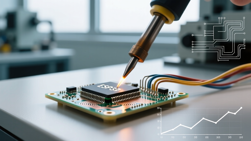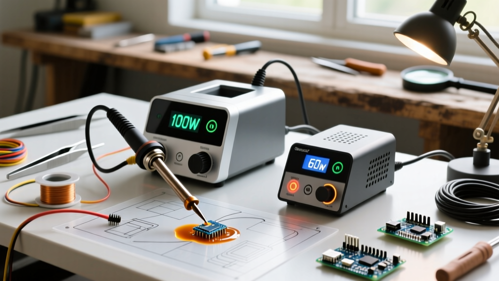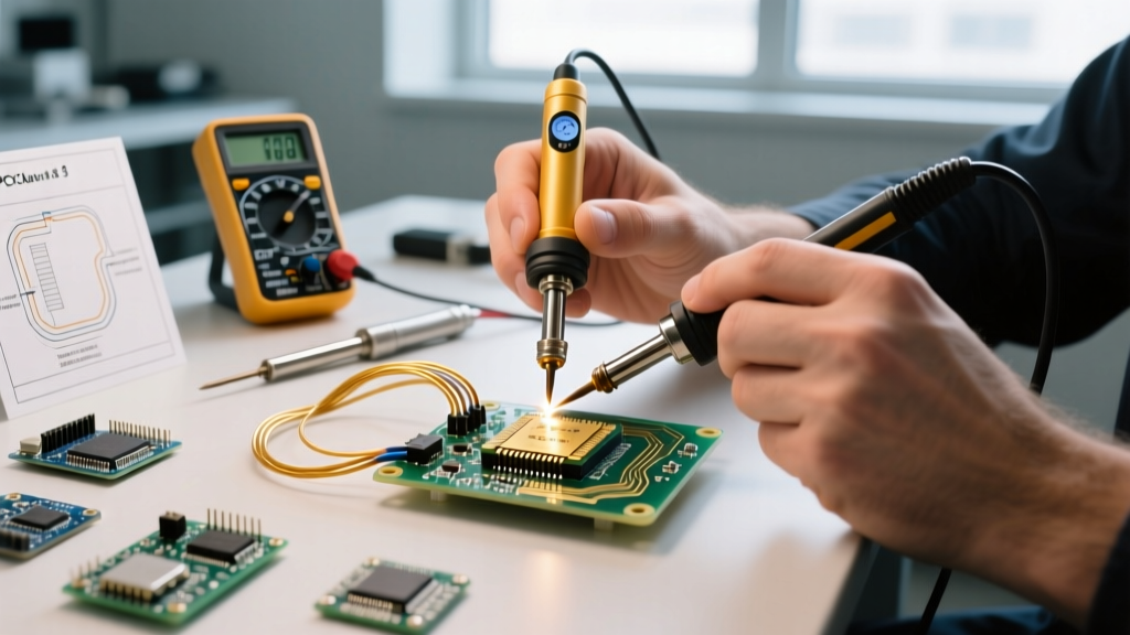

Beyond the Dictionary: The True Industrial Soldering Definition
When most hobbyists and beginners look up the soldering definition, they encounter a simplistic dictionary entry: the process of joining two or more metal items by melting and putting a filler metal into the joint, where the filler metal has a lower melting point than the adjoining metal. While technically accurate for a high school physics class, this basic soldering definition is dangerously incomplete for modern electronics manufacturing, aerospace engineering, and automotive design.
In the professional realm, the industrial soldering definition is rooted in metallurgical science and stringent quality assurance frameworks. It is defined as the controlled formation of an Intermetallic Compound (IMC) between a copper substrate and a tin-based alloy, facilitated by thermal energy and chemical flux, resulting in a joint that guarantees electrical continuity, mechanical shear strength, and long-term thermal fatigue resistance. As we navigate the complex landscape of 2026 electronics manufacturing, understanding this advanced definition is critical for anyone transitioning from DIY prototyping to high-reliability contract manufacturing.
The Core Soldering Definition vs. Industrial Reality
To a hobbyist, a successful solder joint is one that conducts electricity and looks shiny. To a manufacturing engineer operating under IPC-J-STD-001 guidelines, a shiny joint is merely a visual byproduct of proper cooling; the true success is measured in micrometers of IMC growth and the absence of microscopic voids.
The modern industrial definition requires strict adherence to thermal profiles. For example, when using SAC305 (96.5% Tin, 3.0% Silver, 0.5% Copper)—the industry standard lead-free alloy—the liquidus temperature is 217°C. However, the process definition demands a peak temperature of 235°C to 250°C for a specific dwell time (typically 30 to 60 seconds) to ensure proper wetting without degrading the FR-4 laminate or causing pad cratering.
The Role of Flux in the Chemical Definition
You cannot define soldering without defining flux. In industrial applications, flux is not just a cleaning agent; it is a precisely engineered chemical catalyst. Modern no-clean fluxes (like those meeting IPC J-STD-004 Type ROL0) contain specific activators that only become chemically active at precise temperature thresholds, stripping copper oxides just milliseconds before the molten alloy makes contact. This prevents re-oxidation and ensures a pristine metallurgical bond.
How Key Industries Define and Regulate Soldering
The definition of an "acceptable" solder joint shifts dramatically depending on the end-use environment. The NASA Workmanship Standards Program and the IPC divide electronic assemblies into three distinct classes, each with its own functional definition of reliability.
| Parameter | Class 1: General Electronics | Class 2: Dedicated Service | Class 3: High-Performance / Life Support |
|---|---|---|---|
| Target Application | Consumer toys, basic appliances | Computers, telecom, automotive | Aerospace, medical life-support, military |
| Through-Hole Fill Definition | Minimum 50% barrel fill | Minimum 75% barrel fill | 100% barrel fill required (or 75% with specific wetting criteria) |
| Surface Mount Fillet | Wetting visible, minor voids allowed | Continuous fillet, smooth transition | Perfectly concave fillet, zero visible voids, strict heel/toe coverage |
| Thermal Shock Tolerance | Standard room-temp operation | -20°C to +85°C cycling | -55°C to +125°C extreme cycling without IMC fracture |
| Cleaning / Residue | Often ignored | Controlled, non-corrosive | Strictly cleaned or validated no-clean; zero ionic contamination |
Metallurgical Breakdown: What Actually Happens at the Joint
To truly master the industrial soldering definition, one must understand the metallurgy of the joint. When molten tin (Sn) contacts a copper (Cu) pad, they do not simply mix; they react to form distinct Intermetallic Compounds (IMCs).
- Cu6Sn5 (Eta Phase): This scalloped layer forms first at the interface between the bulk solder and the copper. It is relatively ductile and provides the primary mechanical bond.
- Cu3Sn (Epsilon Phase): This planar layer forms between the Cu6Sn5 and the bare copper substrate, especially during prolonged heat exposure or high-temperature aging.
The Goldilocks Zone: The ideal IMC thickness is between 1.0 and 3.0 micrometers. If the soldering iron dwell time is too short, the IMC is too thin, resulting in a weak, cold joint that will fail under mechanical vibration. If the dwell time is too long, or the temperature too high, the Cu3Sn layer grows excessively (beyond 5.0 micrometers). Cu3Sn is highly brittle; an overly thick layer will cause the joint to fracture like glass during thermal expansion and contraction.
Equipment Specifications for 2026 Manufacturing
Achieving the precise thermal control required by the industrial definition is impossible with cheap, transformer-based hobby irons. Modern high-density PCBs feature heavy copper ground planes (2oz to 4oz copper) that act as massive heat sinks. In 2026, professional labs rely on advanced thermal feedback systems.
- Inductive Heating (e.g., Metcal CV-5200): Priced around $750, these stations use RF fields to heat a ferromagnetic core inside the tip. The tip's Curie point physically limits the maximum temperature, providing inherent thermal runaway protection. Ideal for heavy ground planes where constant wattage is required.
- Active-Tip Cartridge Systems (e.g., JBC CD-2BQE): Retailing for approximately $620, JBC systems integrate the heating element directly into the very tip of the cartridge (like the C245 series). This reduces the thermal distance to the joint to mere millimeters, allowing for instantaneous heat recovery when soldering 0402 surface mount components.
Common Failure Modes When Industrial Definitions Are Ignored
When technicians operate under the hobbyist definition of soldering rather than the industrial one, specific, catastrophic failure modes emerge in high-reliability environments.
1. Pad Cratering (Enigma of Lead-Free Alloys)
Lead-free alloys like SAC305 have higher surface tension and require higher processing temperatures. If a technician applies excessive mechanical force with a soldering iron tip while the solder is in a semi-solid state, it can literally tear the copper pad away from the fiberglass laminate beneath it. This is known as pad cratering and is often invisible to the naked eye, only revealing itself during X-ray inspection or operational thermal cycling.
2. Tombstoning in SMT Assembly
In automated reflow soldering, tombstoning occurs when a small surface mount component (like a 0201 resistor) stands on one end. This happens when the solder paste on one pad melts and wets before the other, creating an imbalance in surface tension forces. The industrial definition of a robust soldering process mandates strict stencil aperture reduction and precise thermal profiling to ensure simultaneous melting on both pads.
3. Tin Whisker Growth
Pure tin finishes, often used in RoHS-compliant components, are prone to growing microscopic, conductive crystalline structures known as tin whiskers. These can bridge adjacent pins on a QFP (Quad Flat Package) IC, causing short circuits years after deployment. The industrial mitigation definition requires either the use of tin-lead dips (where legally exempted), the addition of trace bismuth/nickel to the alloy, or the application of specialized polyurethane conformal coatings to physically restrict whisker growth.
Expert Insight: "The transition to lead-free soldering didn't just change the melting point; it fundamentally altered the mechanical definition of a solder joint. SAC305 joints are stiffer and more brittle than traditional Sn63Pb37. In automotive and aerospace applications, we now define reliability not just by thermal stability, but by the joint's ability to absorb mechanical shock without transferring that stress directly to the silicon die." — Advanced Microelectronics Packaging Symposium, Surface Mount Technology Association (SMTA).
Conclusion: Elevating Your Soldering Practice
Understanding the true industrial soldering definition is the dividing line between a tinkerer and a professional electronics engineer. It requires shifting your mindset from simply "melting metal to connect wires" to "engineering a controlled intermetallic bond capable of surviving harsh environmental stressors." By adopting IPC standards, utilizing precision thermal equipment, and respecting the metallurgy of IMC formation, you ensure that your assemblies meet the rigorous demands of modern 2026 technology sectors, from medical devices to deep-space telemetry systems.