
The Metallurgical Dance: A Brief History of PCB Soldering
PCB soldering is often reduced to the simple act of melting metal to join two conductors. In reality, it is a complex metallurgical dance involving capillary action, intermetallic compound (IMC) formation, and precise thermal profiling. As electronic components have shrunk from vacuum tubes to nanometer-scale BGAs, the methods used to attach them have undergone radical transformations. Understanding the history and evolution of PCB soldering is not just an academic exercise; it provides critical context for selecting the right equipment, alloys, and thermal profiles for modern electronics manufacturing and high-end DIY prototyping.
1920s–1950s: Point-to-Point and the Birth of the PCB
Before printed circuit boards existed, electronics relied on point-to-point wiring. Components were mounted on terminal strips, and thick gauge wires were hand-soldered using heavy, high-wattage irons. The concept of the PCB was first patented by Charles Ducas in 1925, but it was Austrian engineer Paul Eisler who created the first functional printed circuit board in 1936 for a valve radio. During World War II, the US military adopted the technology for proximity fuses, utilizing a process called 'Auto-Sembly' where component leads were inserted through holes in a phenolic board and dip-soldered into a bath of molten tin-lead.
These early processes relied heavily on SN63Pb37 (63% Tin, 37% Lead), a eutectic alloy that transitions directly from solid to liquid at exactly 183°C (361°F) without a plastic (pasty) state. This predictable thermal behavior made hand soldering with early Weller and Hakko irons manageable, even with rudimentary temperature control.
1960s–1980s: The Through-Hole Era and Wave Soldering
As consumer electronics boomed in the 1960s, hand-soldering thousands of through-hole joints per board became a manufacturing bottleneck. The solution was the wave soldering machine, pioneered by companies like Electrovert. A wave solder system pumps molten solder upward through a nozzle to create a standing 'wave'. The PCB, populated with through-hole components, is passed over this wave on a conveyor.
The process requires strict orchestration:
- Fluxing: Rosin-based or water-soluble flux is sprayed onto the board's underside to remove oxidation.
- Preheating: Infrared or convection heaters raise the board's temperature to 90°C–130°C to activate the flux and prevent thermal shock.
- Wave Contact: The board hits the 235°C–250°C solder wave for 2 to 4 seconds. Capillary action pulls the solder up through the plated through-holes (PTH).
'The invention of the wave soldering machine in the mid-20th century was the catalyst that allowed consumer electronics to scale from bespoke laboratory instruments to mass-produced household commodities.' — Historical archives from the Surface Mount Technology Association (SMTA).
1980s–2000s: The Surface Mount (SMT) Revolution
Through-hole components were bulky and required drilling thousands of holes, weakening the FR-4 fiberglass substrate. In the 1980s, Surface Mount Technology (SMT) emerged, championed by IBM. SMT components (resistors, capacitors, and early ICs) featured short leads or metalized terminations that sat directly on copper pads.
Wave soldering was unsuitable for most SMT parts, giving rise to reflow soldering. The modern reflow process involves:
- Stencil Printing: A laser-cut stainless steel stencil is used to apply Type 3 or Type 4 solder paste (a mixture of microscopic solder spheres and tacky flux) onto the pads.
- Pick-and-Place: Pneumatic nozzles place SMT components onto the tacky paste.
- Reflow Oven: The board passes through a multi-zone convection oven following a specific thermal profile.
The standard 'Ramp-Soak-Spike' profile became the industry standard. The soak zone (150°C–190°C for 60–90 seconds) allows the flux to clean the pads and equalize temperatures across the board, preventing tombstoning (where surface tension pulls a component upright). The spike zone pushes the assembly above the solder's liquidus temperature (typically 215°C–230°C for leaded pastes) to form the copper-tin intermetallic bond.
2006–Present: The RoHS Directive and the Lead-Free Shock
The most disruptive event in the history of PCB soldering was the European Union's Restriction of Hazardous Substances (RoHS) Directive, fully enforced in 2006. The mandate to eliminate lead (Pb) from consumer electronics forced the industry to adopt lead-free alloys, primarily SAC305 (96.5% Tin, 3.0% Silver, 0.5% Copper).
The Thermal and Metallurgical Toll
SAC305 has a melting point of 217°C, requiring peak reflow temperatures of 245°C–260°C. This 40°C+ increase caused massive engineering headaches:
- FR-4 Delamination: Standard FR-4 PCBs have a Glass Transition Temperature (Tg) of around 135°C–150°C. The extreme heat of lead-free reflow caused boards to warp, blister, and suffer from pad cratering.
- Tin Whiskers: Pure tin finishes, used as a lead-free alternative on component leads, are prone to growing microscopic, conductive 'whiskers' that can cause catastrophic short circuits in high-reliability systems. The NASA Electronic Parts and Packaging (NEPP) Program has extensively documented tin whisker failures in aerospace applications, leading to strict mitigation standards.
- Component Stress: Electrolytic capacitors and plastic-bodied ICs frequently cracked or degraded under prolonged exposure to 260°C.
Modern Frontiers: Selective Wave, Vapor Phase, and Laser
Today, PCB soldering has fractured into highly specialized niches to handle complex, mixed-technology boards (boards with both fine-pitch SMT and heavy power through-hole connectors).
- Selective Wave Soldering: Machines like the Kurtz Ersa POWERFLOW use programmable, miniature solder nozzles to solder specific through-hole pins without exposing nearby SMT components to the molten wave.
- Vapor Phase Soldering: Utilizing inert fluorocarbon fluids (like Galden) that boil at precise temperatures (e.g., 230°C), vapor phase systems create an oxygen-free environment. The condensation of the vapor on the board provides perfectly uniform heating, making it the gold standard for high-density aerospace and medical PCBs.
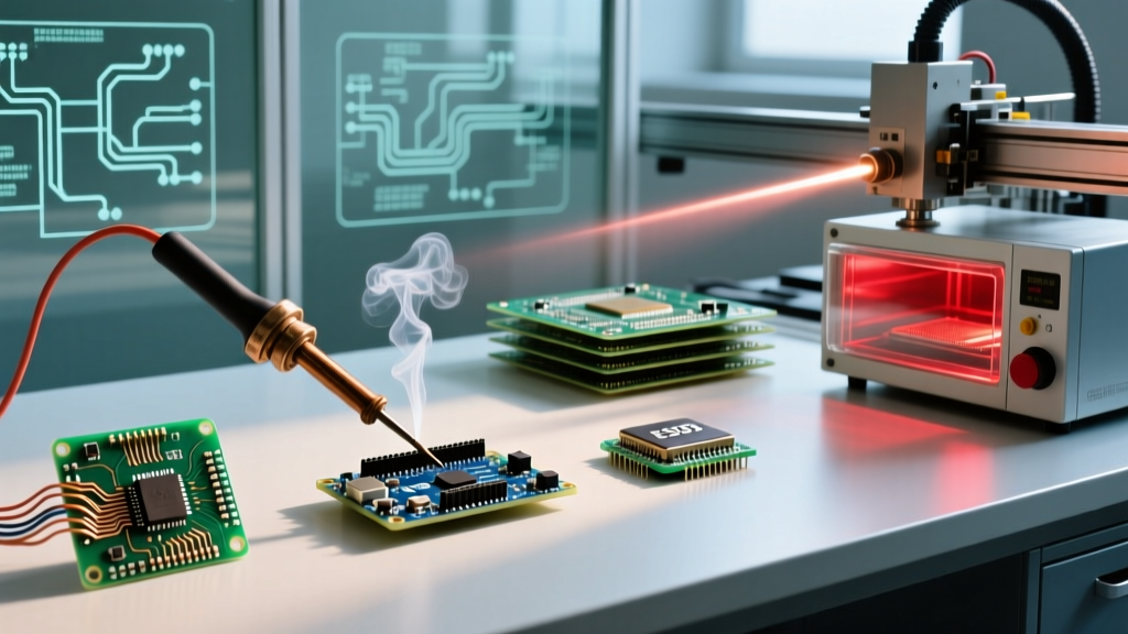
- Laser Soldering: For heat-sensitive components, micro-BGAs, or flexible PCBs (flex circuits), diode laser systems (such as those from Finetech) deliver pinpoint thermal energy in milliseconds, eliminating the thermal spread that damages adjacent traces.
Evolution of Solder Alloys & Thermal Profiles
The following table illustrates how the dominant alloys and thermal requirements have shifted over the decades, directly impacting the equipment required on the workbench and the factory floor.
| Era | Dominant Technology | Standard Alloy | Liquidus Temp | Peak Process Temp | Primary Defect Risk |
|---|---|---|---|---|---|
| 1950s–1980s | Hand / Wave Soldering | SN63Pb37 (Leaded) | 183°C | 235°C–250°C | Cold joints, bridging |
| 1980s–2005 | SMT Reflow (Leaded) | SN62Pb36Ag2 | 179°C | 215°C–230°C | Tombstoning, solder balls |
| 2006–Present | SMT Reflow (Lead-Free) | SAC305 | 217°C | 245°C–260°C | Pad cratering, voiding, head-in-pillow |
| 2015–Present | Low-Temp / Biomedical | Sn42Bi58 | 138°C | 160°C–180°C | Brittle joints, bismuth leaching |
What This History Means for Your Workbench Today
When purchasing a soldering station in 2026, historical context dictates your hardware requirements. If you are exclusively repairing vintage audio equipment or assembling heavy through-hole power supplies, a standard 70W station like the Hakko FX-951 is perfectly adequate for melting SN63Pb37 or even thicker lead-free wires.
However, if you are prototyping modern SMT boards, reworking 0402 passives, or dealing with high-thermal-mass ground planes using SAC305, you need rapid thermal recovery. Stations utilizing cartridge-based heaters—where the heating element and tip are a single integrated unit—are mandatory. The JBC CD-2BQF (using C245 handles) delivers 350W peak power and recovers from a 250°C temperature drop in under two seconds, preventing the pad cratering and cold joints that plagued early lead-free adopters. Furthermore, adhering to the guidelines set forth by the IPC (Association Connecting Electronics Industries), specifically IPC-J-STD-001 and IPC-A-610, ensures that whether you are using a $50 iron or a $5,000 laser system, your intermetallic bonds meet modern reliability standards.
The evolution of PCB soldering is a testament to the industry's ability to adapt to environmental mandates and miniaturization demands. By respecting the metallurgy and thermal dynamics developed over the last century, modern engineers and DIYers can achieve factory-grade reliability on their own workbenches.