
The Physics of Thermal Transfer in High-Reliability Assembly
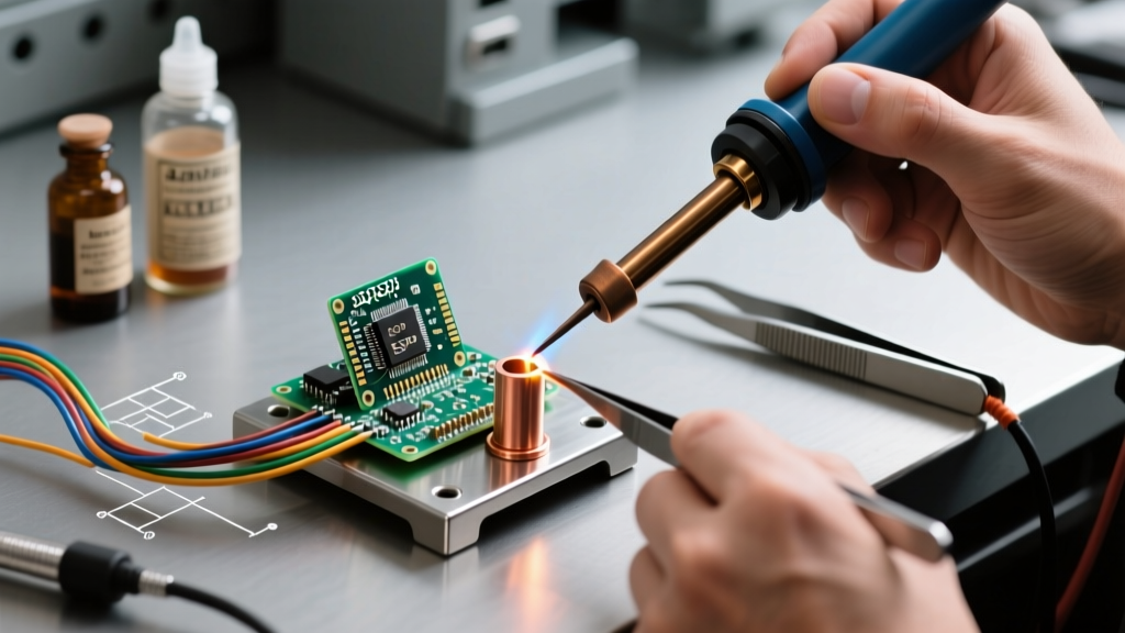
In industrial electronics manufacturing and aerospace prototyping, determining the best temp for soldering is never a matter of picking a single static number. It is a dynamic calculation involving alloy metallurgy, component thermal mass, and the strict wetting requirements mandated by IPC J-STD-001 for Class 3 (High Performance) assemblies. A static dial setting of 350°C on a soldering station does not guarantee the solder joint itself reaches 350°C; in fact, on a multi-layer board with heavy copper pours, the actual joint temperature may stall at 210°C, resulting in a catastrophic cold joint.
For industrial applications, thermal management is about optimizing the heat transfer rate (Joules per second) from the tip to the pad, through the component lead, and into the solder paste or wire, without exceeding the Glass Transition Temperature (Tg) of the FR-4 laminate or damaging silicon die internals.
Decoding the Best Temp for Soldering Across IPC Alloy Classes
The baseline temperature profile is dictated entirely by the metallurgical composition of the solder alloy. Different industries mandate different alloys based on environmental stress, vibration, and RoHS compliance. Below is the definitive thermal matrix for industrial applications.
| Alloy Designation | Composition | Melting Point (°C) | Optimal Tip Temp (°C) | Primary Industry Application |
|---|---|---|---|---|
| SAC305 | Sn96.5/Ag3.0/Cu0.5 | 217 - 220 | 320 - 350 | Medical, Automotive, Consumer |
| Sn63/Pb37 | Sn63/Pb37 | 183 (Eutectic) | 280 - 310 | Aerospace, Military, Legacy |
| SAC405 | Sn95.5/Ag4.0/Cu0.5 | 217 - 221 | 330 - 360 | High-Vibration Automotive |
| Sn10/Pb88/Ag2 | Sn10/Pb88/Ag2 | 268 - 299 | 360 - 390 | Downhole Drilling, Well-Logging |
SAC305 (Lead-Free) Industrial Profiles
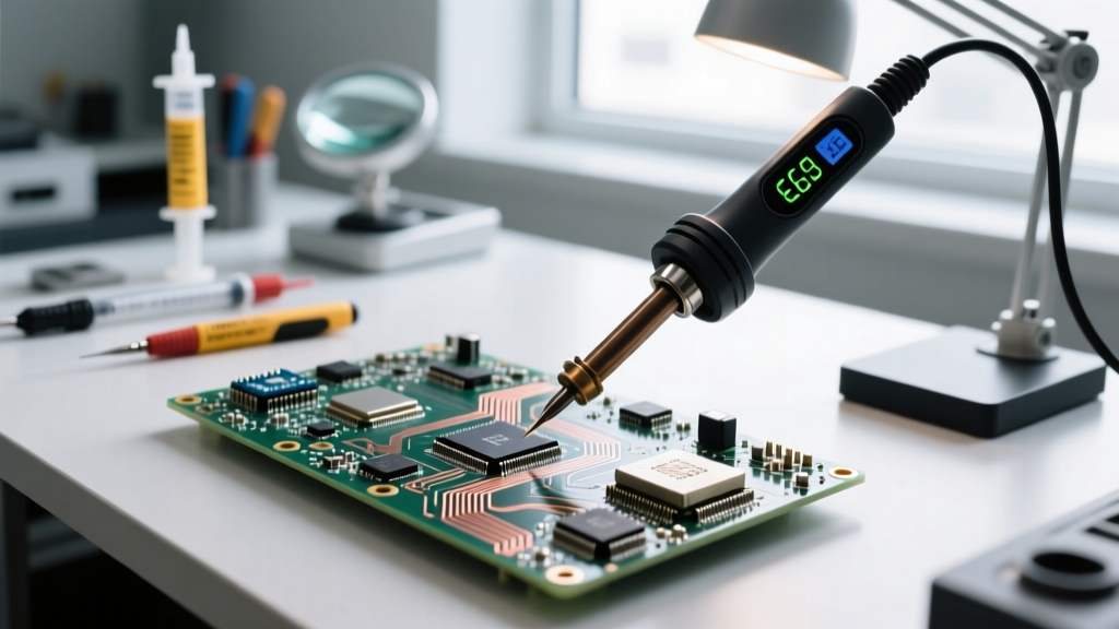
SAC305 is the undisputed standard for modern commercial and medical electronics. Because its liquidus point sits at 220°C, the iron tip must operate at a minimum delta of +100°C above the melting point to ensure rapid wetting and proper Intermetallic Compound (IMC) formation. Setting your station to 340°C is generally the sweet spot for standard 0603 and 0805 SMD components, as well as through-hole DIP ICs.
Sn63/Pb37 (Leaded) Aerospace & Legacy Profiles
Under NASA Electronic Parts and Packaging (NEPP) guidelines and military exemptions, leaded solder remains critical due to its resistance to tin whiskers. The eutectic Sn63/Pb37 alloy melts sharply at 183°C. The best temp for soldering this alloy in high-reliability aerospace environments is strictly between 280°C and 310°C. Exceeding 330°C with leaded solder accelerates flux burn-off and increases the risk of lifting copper pads on older, polyimide-based flex circuits.
Calibrating for Thermal Mass: Component vs. Ground Plane
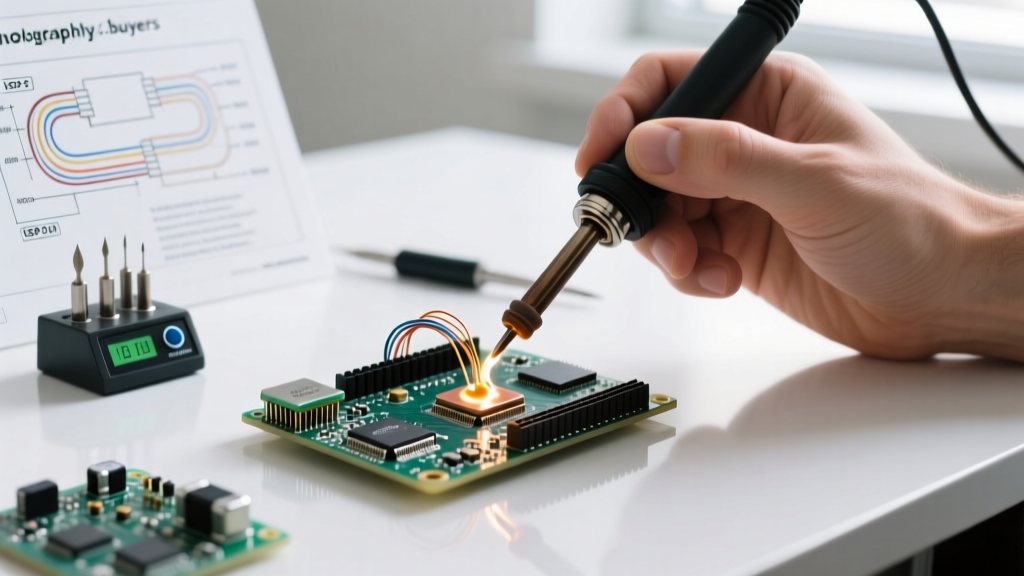
The most common failure in industrial hand soldering occurs when technicians apply a baseline temperature to a high-thermal-mass joint. A 10-layer PCB featuring 2oz copper ground planes acts as a massive heat sink. If you apply a standard 2.4mm chisel tip at 340°C to a through-hole capacitor grounded to an internal plane, the heat will dissipate into the board faster than the iron can supply it.
The Thermal Mass Offset Rule: Never compensate for high thermal mass by simply increasing the station temperature past 380°C. This will instantly oxidize the tip plating and scorch the flux activators. Instead, increase the surface area of the tip (e.g., switching to a JBC C245-118 heavy-duty chisel or a Pace Blue Tip) and raise the temperature by a maximum of 20°C to 30°C to drive higher thermal transfer (Watts) without exceeding the thermal degradation limits of the board laminate.
Industry-Grade Equipment: Maintaining the Target Curve
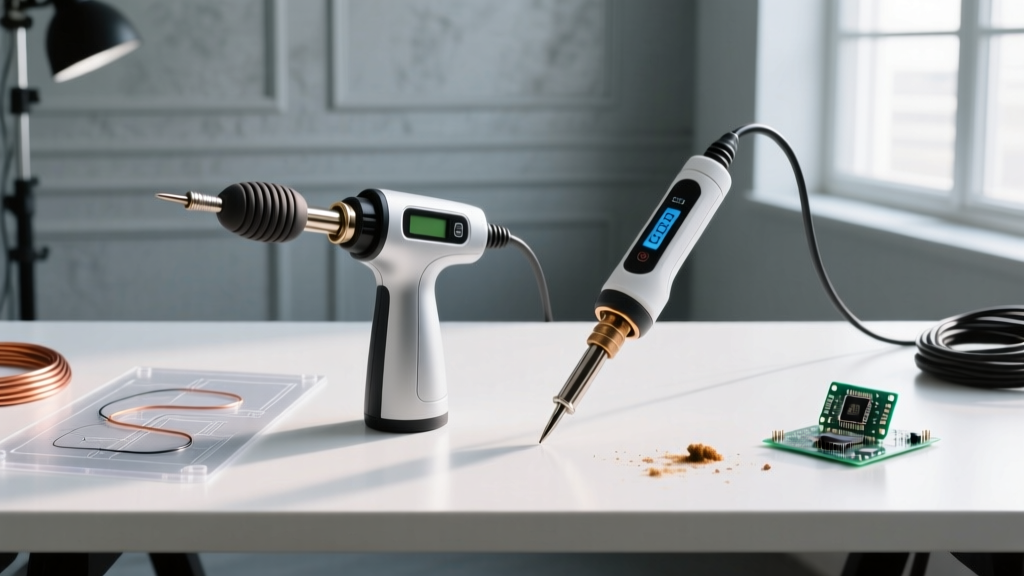
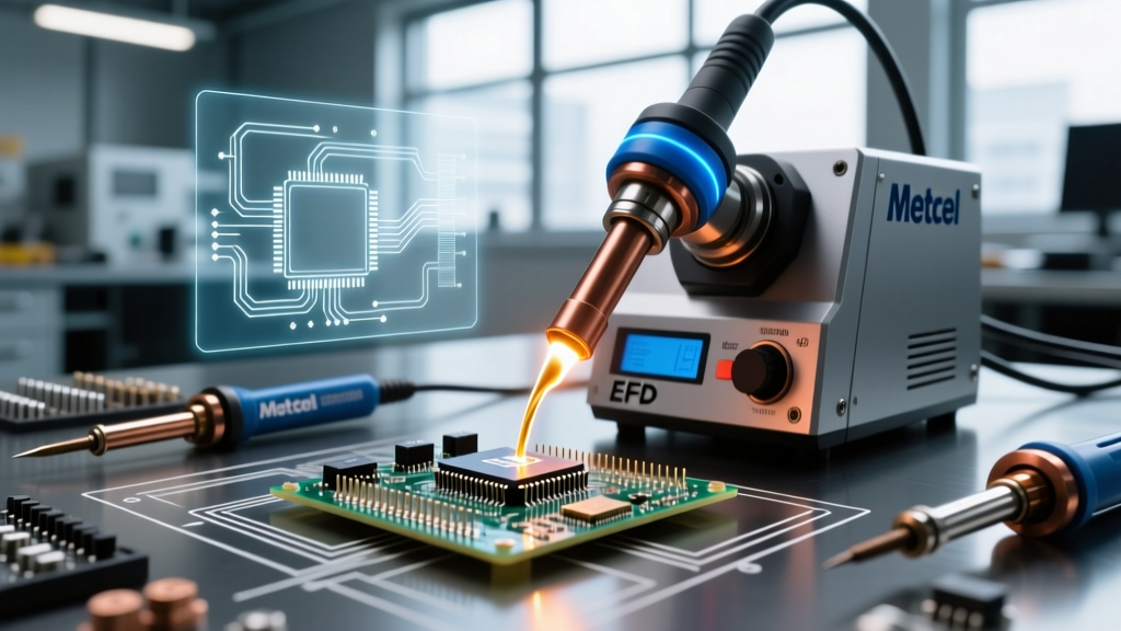
Achieving the exact thermal profile requires equipment with sub-second thermal recovery rates. In 2026, industrial floors rely on active-cartridge systems rather than traditional ceramic heater wands.
- JBC CD-2BQE (Approx. $685): The industry benchmark for precision. The heating element is integrated directly into the cartridge tip. When a high-mass joint draws heat, the JBC station detects the temperature drop and delivers 130W of power, recovering to 350°C in under 2 seconds. This prevents the operator from lingering on the pad, which is a primary cause of delamination.
- Weller WX2021 (Approx. $890): Features a 150W power unit and RT micro-tips. The WX series excels in IoT and dense RF assemblies where operators must transition rapidly between a 0201 resistor (requiring low thermal transfer) and an RF shield ground lug (requiring high thermal transfer). The GUI allows locking specific temperature profiles per operator badge to maintain IPC compliance.
- Pace TF 2700 (Approx. $550): Utilizes ThermoDrive technology. It is highly favored in heavy industrial and automotive ECU rework where thick copper layers require sustained, aggressive heat delivery without tip degradation.
Failure Modes from Thermal Mismanagement
Deviating from the optimal thermal envelope introduces specific, quantifiable failure modes that will fail X-ray or Automated Optical Inspection (AOI):
- Excessive Intermetallic Compound (IMC) Growth: The bond between solder and copper relies on a Cu6Sn5 IMC layer. Ideally, this layer should be 1 to 2 microns thick. If the tip temperature is too high (e.g., >380°C for SAC305) or dwell time exceeds 4 seconds, the IMC layer grows into a thick, brittle Cu3Sn structure. Under thermal cycling or mechanical shock, the joint will fracture along this boundary.
- Flux Activator Depletion: Modern no-clean fluxes contain carboxylic acid activators designed to vaporize precisely as the solder reaches its liquidus state. If the iron is too cool, the solder melts before the flux activates, resulting in severe oxidation, icicles, and solder bridging on fine-pitch QFPs.
- Laminate Delamination (Measling): Standard FR-4 has a Tg of 130°C to 170°C. Prolonged exposure to a struggling, low-temperature iron causes the resin matrix to expand and separate from the glass weave, visible as white 'measling' spots around the via barrels.
- Silicon Die Cracking: For large BGA or QFN components, applying excessive localized heat to one corner creates a severe thermal gradient across the silicon die or ceramic substrate, leading to micro-fractures that manifest as intermittent field failures.
Validating Your Thermal Profile in Production
In a regulated industrial environment, assuming the station's digital readout is accurate is a violation of quality assurance protocols. To validate the actual thermal curve at the joint level, engineers must perform a physical thermal profile test.
Attach a K-type thermocouple (using high-temperature Kapton tape or a dab of UV-cure thermal adhesive) directly to the component lead and the adjacent PCB pad. Connect the thermocouple to a data logger (such as the PACE SRT-100 or an equivalent Fluke industrial logger). Apply the iron using the intended production tip and technique. The resulting time-temperature graph must show the joint reaching the alloy's liquidus point +20°C within 2 to 3 seconds, and the total time above liquidus (TAL) must not exceed 5 seconds to comply with IPC-A-610 Class 3 workmanship standards.
By treating temperature not as a static dial setting, but as a dynamic variable governed by alloy chemistry and thermal mass, manufacturing teams can eliminate latent solder defects and guarantee long-term field reliability.