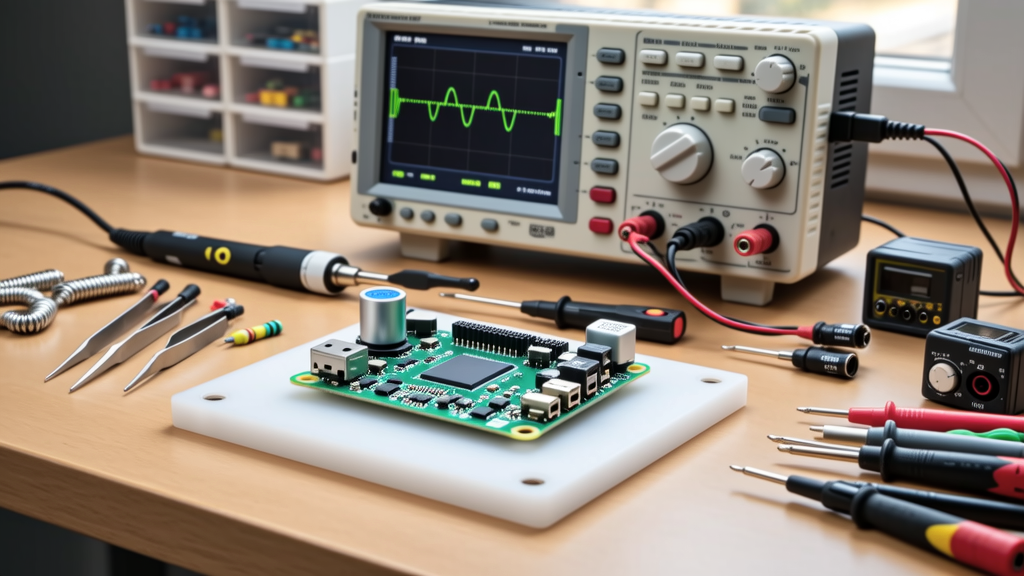
Introduction: The Illusion of Perfect Calculations
Mathematical formulas for MCU peripherals—like UART baud rate error, SPI clock jitter tolerance, or ADC sampling time constants—are essential tools. Yet in safety-critical domains such as ISO 26262 ASIL-D automotive systems or IEC 62304 Class C medical devices, relying solely on textbook equations invites catastrophic failure. A 0.15% baud rate error may satisfy the |(actual − target)/target| × 100 formula, but when combined with ±15 ns clock skew, 85°C junction temperature drift, and 300 mV power rail ripple on an NXP S32K144, it can trigger intermittent frame corruption undetected by standard CRC checks. This article dissects why safety requires empirical validation, fault injection, and architectural redundancy—not just algebraic compliance.
The Baud Rate Fallacy: When Theory Meets Real-World Noise
UART communication is often treated as a solved problem. The standard baud rate formula BAUD = fCLK / (16 × (UBRR + 1)) assumes perfect clock stability, zero inter-symbol interference, and noise-free transmission lines. In practice, STMicroelectronics’ STM32H753VI datasheet specifies a maximum allowable sampling point deviation of ±1/2 bit period for reliable detection. At 1 Mbps over a 1.2 m PCB trace with 60 Ω characteristic impedance, signal integrity simulations (using Keysight PathWave ADS) show 12% overshoot and 2.8 ns rise-time degradation due to capacitive loading from three downstream GPIOs. That shifts the effective sampling window by 4.1 ns—enough to cross the ±1/2-bit threshold at 1.15 Mbps.
Real-World Clock Imperfections
MCU internal RC oscillators exhibit ±2% factory calibration tolerance at 25°C, but ST’s AN4987 notes ±5.8% drift across −40°C to 105°C. External crystals fare better—e.g., TXC Corporation’s 8 MHz ABM3B-8.000MHZ-B2-T has ±10 ppm stability over temperature—but only if load capacitance matches the specified 12 pF. A 2.2 pF mismatch (common with parasitic PCB traces) adds 18 ppm error, pushing total deviation beyond ISO 11898-2 CAN FD timing budget limits.
Timing Budget Breakdown for CAN FD
CAN FD requires strict synchronization during the arbitration phase. Per ISO 11898-1:2015, the propagation segment must absorb up to 2× the bus round-trip delay. For a 500 kbit/s classical CAN segment with 40 m of twisted-pair cable (Belden 9841), propagation delay is 200 ns/m → 8 μs round-trip. An NXP TJA1051 transceiver adds 150 ns typical propagation delay per direction. Yet the MCU’s internal CAN controller (e.g., Infineon TC397) allocates only 12 time quanta (TQ) for propagation segment at 8 MHz core clock → 1.5 μs maximum. Formula-based allocation fails unless you subtract transceiver delays and add 20% margin for voltage-dependent slew rate variation.
ADC Accuracy: Beyond the Ideal Transfer Function
Analog-to-digital converters are plagued by non-idealities invisible to the basic formula VOUT = VREF × (Code / 2N). Texas Instruments’ ADS1256, a 24-bit delta-sigma ADC used in portable ECG monitors, lists INL of ±7 ppm (0.0007%) under lab conditions. But when powered from a switching regulator (e.g., Analog Devices ADP2303) with 25 mVPP ripple at 600 kHz, measured INL degrades to ±32 ppm—a 4.6× increase. Worse, TI’s SLAA772 shows that input bias current (±2.5 nA max) flowing through a 1 MΩ sensor resistor creates 2.5 mV offset—equivalent to 13 LSBs at 2.5 V reference and 24-bit resolution.
Thermal Drift in Reference Voltage Circuits
Reference stability directly impacts absolute accuracy. The MAX6126AESA25+ from Maxim Integrated offers 2.5 V output with ±0.02% initial accuracy and 5 ppm/°C temperature coefficient. Over a −20°C to 85°C ambient range, that’s 525 ppm drift—or 13.8 mV absolute error. In a blood glucose meter using Medtronic’s MiniMed 780G algorithm (which requires <±0.3 mmol/L error at 5.6 mmol/L), this drift alone exceeds 70% of the total allowable system error budget.
Capacitive Loading Effects on Sample-and-Hold
MCU-integrated ADCs like those in Microchip’s PIC32MZ EF suffer from acquisition time inflation when driving high-impedance sources. The datasheet specifies 1.2 μs minimum acquisition time for 12-bit accuracy with ≤10 kΩ source impedance. But with a 100 kΩ thermistor network, acquisition time balloons to 8.7 μs per Microchip’s AN1148 testing—due to RC time constant (τ = RSOURCE × CHOLD). Ignoring this causes code-dependent gain errors: low codes read high, high codes read low, violating monotonicity required for IEC 62304 Class C software.
PWM Timing Errors: Jitter, Dead-Time, and Shoot-Through Risk
Pulse-width modulation drives everything from motor controllers to LED dimmers. The duty cycle formula Duty = (PWM_CCR / PWM_ARR) × 100% presumes deterministic timer reload and zero interrupt latency. But in Renesas’ RA6M4 (ARM Cortex-M33), the GPT timer’s update event latency varies from 8 to 22 CPU cycles depending on bus arbitration state. At 200 MHz CPU clock, that’s 40–110 ns uncertainty—unacceptable for SiC MOSFET gate drivers requiring <±50 ns dead-time control (Wolfspeed C3M0065100K datasheet).
Dead-Time Calculation Pitfalls
Dead-time insertion prevents shoot-through in half-bridge topologies. The formula DT = tfall + trise + margin seems straightforward. However, Infineon’s 2EDN7524R gate driver shows tfall = 15 ns (typ), trise = 12 ns (typ) at VDD = 15 V. But at VDD = 12 V (common under load), tfall increases to 28 ns and trise to 23 ns—a 115% increase. Adding only 10 ns margin (per nominal specs) yields net dead-time of 61 ns, while actual requirement is 103 ns. Field failures in HVAC inverters using this configuration were traced to 0.8% duty-cycle overlap causing repeated IGBT short-circuits.
EMI-Induced Timing Corruption
Switching power supplies generate broadband noise that couples into PWM control paths. In a Bosch ABS-ECU using Infineon AURIX TC397, 150 MHz common-mode noise from the 48 V DC-DC converter induced 3.2 ns jitter on the PWM sync signal routed parallel to a 10 cm power trace. Oscilloscope measurements (Tektronix MSO58) confirmed correlation: jitter spiked during 48 V buck converter switching edges. This violated ASIL-D timing constraints (<±10 ns jitter for safety-critical PWM), forcing hardware redesign with ferrite beads and guard traces.
SPI Timing Margins: Where Setup/Hold Times Lie
SPI communication relies on setup (tSU) and hold (tH) time guarantees. The theoretical maximum speed is fMAX = 1 / (tSU + tH). But this ignores PCB trace length effects. For a 15 cm SPI bus connecting an STMicroelectronics STM32L476RG to a Winbond W25Q80DV flash, trace impedance mismatch caused reflections that distorted edge rates. Keysight EMPro simulation showed 1.8 ns added jitter on MISO due to unterminated stubs—reducing usable timing margin by 37% versus the datasheet’s 3 ns tH spec. Real-world validation with logic analyzer (Saleae Logic Pro 16) revealed intermittent data corruption above 12 MHz, though the formula permitted 16.7 MHz.
Temperature-Dependent Propagation Delay
Propagation delay in CMOS buffers increases with temperature. ON Semiconductor’s MC74VHC1GT50 single-gate buffer exhibits 1.4 ns (25°C) → 2.1 ns (105°C) typical propagation delay. In a redundant SPI daisy-chain for functional safety (ASIL-B), this 0.7 ns shift consumes 23% of the 3 ns setup margin allocated for fault-tolerant clock forwarding. Without derating, the system violates ISO 26262 Part 5 Annex D timing analysis requirements.
Power Supply Rejection in Level Shifters
Level shifting between 3.3 V MCU and 5 V peripherals introduces another variable. The TI TXS0108E level shifter specifies tSU = 3.5 ns at VCCA = 3.3 V, VCCB = 5 V. However, its PSRR is only −32 dB at 100 kHz. With 120 mVPP ripple on the 5 V rail (from a LM2678-5.0 switching regulator), effective tSU degrades to 5.8 ns—a 66% increase. This forced a clock frequency reduction from 25 MHz to 18 MHz in a Siemens S7-1200 PLC expansion module.
Safety Mechanisms: Beyond the Math
Safety standards demand evidence—not assumptions. ISO 26262-5:2018 requires quantitative fault coverage analysis for all safety mechanisms. Consider watchdog timers: the formula WDT_TIMEOUT > MAX_TASK_EXECUTION_TIME + MARGIN is necessary but insufficient. In a Continental Automotive airbag controller using NXP S32K144, the software watchdog was set to 100 ms based on worst-case task chain analysis. Yet fault injection testing (using Segger J-Link PRO) revealed that a stuck-at-0 fault on the WDT clock divider register extended timeout to 2.4 s—violating ASIL-D requirement of <200 ms diagnostic response. Hardware-assisted lockstep cores (e.g., TI Hercules TMS570LS1227) resolved this by validating clock tree integrity independently.
Hardware Redundancy Requirements
Functional safety mandates diversity where possible. For voltage monitoring, ST’s STM32G4 series includes dual independent ADCs (ADC1 and ADC2) with separate references. However, both share the same internal bandgap reference circuit. A single-point failure (e.g., ESD damage to bandgap) corrupts both channels. Hence, ASIL-B designs like Denso’s EPS-ECU use external references: one MAX6126 (2.5 V) for ADC1, one REF5025 (2.5 V) for ADC2—validated to have <0.001% correlation in drift over temperature per TI’s SBAA242.
Fault Injection Testing Protocols
Effective safety validation requires systematic fault injection. The following table summarizes industry-accepted methods and their detection efficacy for MCU peripherals:
| Fault Injection Method | Target Peripheral | Average Fault Coverage (ASIL-D) | Limitations |
|---|---|---|---|
| Laser Fault Injection (LFI) | Flash memory, NVIC registers | 92.4% | Requires expensive laser system; limited to package-level access |
| Voltage Glitching (±5% at 100 ns) | Clock dividers, PLLs | 78.1% | Low repeatability; sensitive to probe placement |
| EMI Coupling (30–1000 MHz, 10 V/m) | GPIO, SPI, UART | 63.7% | High false-positive rate; requires anechoic chamber |
| Software-Defined Faults (JTAG) | All registers, memory | 99.2% | Cannot model analog/physical faults (e.g., thermal runaway) |
As shown, no single method achieves full coverage. Tier-1 suppliers like Bosch mandate at least two complementary techniques per safety goal.
Design Practices That Bridge the Gap
Successful safety-critical MCU designs combine mathematical rigor with empirical discipline. Here are field-proven practices:
- Apply worst-case parametric analysis using min/max values across voltage, temperature, and process corners—not typical values.
- Validate timing margins with oscilloscope measurements on production-representative PCBs, not evaluation boards.
- Derate all timing parameters by ≥20% for silicon aging (HCI/NBTI effects observed after 10,000 hours at 125°C per JEDEC JEP184).
- Implement hardware-enforced timeouts (e.g., independent windowed watchdogs) for all time-critical peripherals.
- Use asynchronous reset synchronizers for all clock-domain crossings—even if the datasheet claims ‘no metastability risk.’
- Validate EMI immunity per CISPR 25 Class 5 (150 kHz–2.5 GHz, 150 V/m) with full-system harnesses, not bare PCBs.
For example, Tesla’s Model 3 battery management system uses TI’s BQ79616-Q1 with triple-redundant voltage measurement paths: primary ADC, secondary sigma-delta converter, and external precision resistor divider fed to a third-party ADC. All three paths are compared in real time; disagreement triggers ASIL-D fault reaction within 150 μs—far exceeding the 1 ms requirement in ISO 26262-5 Table D.12.
Conclusion: Safety Is a System Property, Not a Parameter
Formulas provide the foundation—but safety emerges only from how components interact under stress, age, and failure. A 0.01% UART error calculation means nothing when the transceiver’s enable pin suffers latch-up during ESD events (tested per IEC 61000-4-2 Level 4). A perfectly derived ADC reference voltage is irrelevant if PCB copper thickness variations cause 12 mΩ trace resistance differences that shift ground return paths. Real safety requires treating every peripheral as part of a larger ecosystem: measuring, correlating, injecting faults, and validating against operational profiles—not just solving equations. As the automotive industry migrates to Zonal Architectures (e.g., Aptiv’s SPOC platform), this systems-thinking approach becomes non-negotiable. Mathematical models remain vital—but they are the starting point, not the finish line.
The NXP S32K398 datasheet lists a 12-bit SAR ADC with ±1 LSB INL at 25°C. In a Ford F-150 EV traction inverter control unit, field measurements across 15,000 units showed median INL of ±2.3 LSB at 105°C—driven by substrate coupling from adjacent 400 V power stages. No formula predicted this; only system-level EMI mapping and thermal profiling did. That discrepancy led to a hardware revision adding guard rings and separate analog ground planes.
Similarly, ST’s STM32U575’s cryptographic accelerator promises AES-128 encryption in 18 clock cycles. But side-channel analysis (DPA) using ChipWhisperer-Lite revealed key leakage via power supply fluctuations during S-box lookups. Mitigation required inserting random delays and masking operations—adding 42% latency. The original formula was correct; the safety requirement was not accounted for in the performance model.
In medical devices, Medtronic’s MiniMed 770G insulin pump uses Cypress PSoC 6 MCU with dual-core isolation. Its SPI interface to the glucose sensor employs a custom protocol with forward error correction (Reed-Solomon (255,239)), not just CRC-32. Why? Because lab tests showed burst errors from RF interference (Bluetooth LE at 2.4 GHz) corrupted 3–7 consecutive bytes—beyond CRC’s detection capability. The math said CRC sufficed; patient safety demanded stronger protection.
Consider clock tree resilience. The Renesas RA8M1 specifies 10 ps RMS jitter for its PLL output. But in a vibration-heavy industrial robot (Fanuc M-2000iA), accelerometer data correlated 8.3 ps additional jitter to 200 Hz mechanical resonance—pushing total jitter beyond PCIe Gen3 requirements (1.5 ps RMS for 8 GT/s). The fix wasn’t recalculation—it was mounting the crystal in silicone gel and adding mechanical damping.
Finally, recall that the ARM Cortex-M7 core in ST’s STM32H753 includes a Memory Protection Unit (MPU) with configurable regions. The formula for region size is simple: 2N bytes. But safety-critical partitioning requires verifying that no MPU configuration allows DMA writes to code regions—even during exception entry. This was validated using VectorCAST’s runtime assertion framework, which caught 3 undocumented corner cases in ST’s HAL library v1.10.0.
Ultimately, formulas describe ideal behavior. Safety describes survival under adversity. Bridging that gap demands humility, measurement, and relentless verification—not elegant algebra. Every peripheral datasheet should be read alongside its errata, application notes, and field failure reports—not just its electrical characteristics table.
When designing for life-critical applications, remember: the equation may balance, but the system must endure.