
The Anatomy of a Microcontroller GPIO Pinout
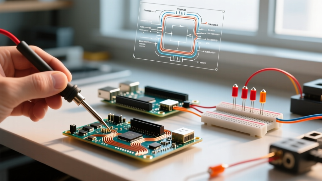
When transitioning from simple LED blink sketches to complex sensor networks, the first major hurdle every maker faces is understanding the GPIO pinout of their chosen microcontroller. A General Purpose Input/Output (GPIO) pinout diagram is essentially the Rosetta Stone of embedded systems, translating physical silicon connections into software-addressable logic. However, reading these diagrams requires navigating a maze of silkscreen labels, logical pin numbers, and alternate hardware functions.
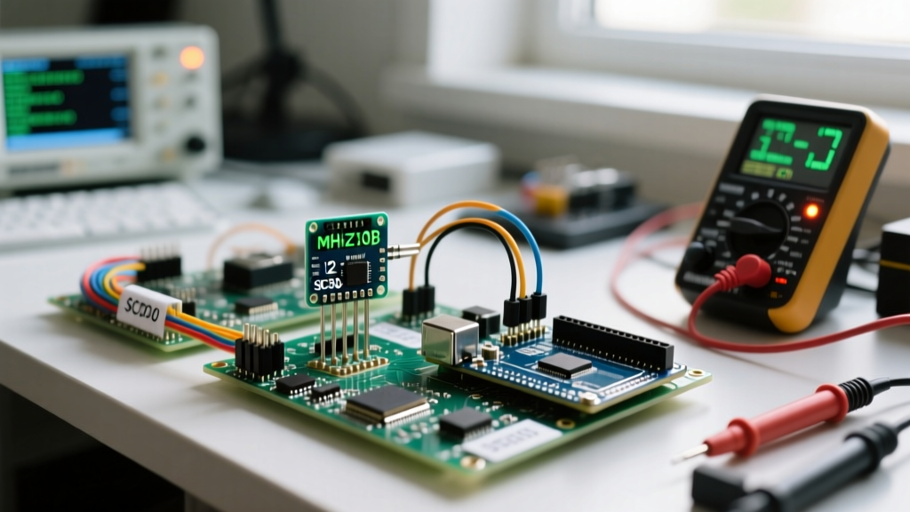
The most common point of failure for beginners is confusing the physical silkscreen label on a development board with the actual GPIO number used in code. For example, on the popular NodeMCU ESP8266 board, the silkscreen reads D4. Many beginners write digitalWrite(D4, HIGH) in their Arduino IDE sketch, only to find the wrong pin activating. In reality, D4 on the NodeMCU silkscreen maps to GPIO2 on the underlying ESP8266 silicon. Modern ESP32 DevKit boards largely avoid this by printing the raw GPIO numbers (e.g., 23, 19) directly on the PCB, but understanding the distinction between board-level mapping and silicon-level mapping is critical for reading any schematic or pinout diagram accurately.
Voltage Logic and Current Limits: The Hidden Dangers
A pinout diagram is not just a functional map; it defines the strict electrical boundaries of your microcontroller. Ignoring the voltage and current specifications associated with specific GPIO pins is the fastest way to permanently brick a development board.
The ATmega328P (found in the Arduino Uno R3) operates on 5V logic. Its GPIO pins can safely source or sink up to 20mA continuously, with an absolute maximum rating of 40mA. In contrast, modern 32-bit microcontrollers like the ESP32 and the Raspberry Pi Pico (RP2040) operate on 3.3V logic. Connecting a 5V sensor output directly to an ESP32 GPIO pin without a logic level shifter will overvoltage the internal ESD protection diodes, causing excessive current to flow into the 3.3V rail and potentially destroying the SoC.
Sourcing vs. Sinking Current
Pinout diagrams often note current limits, but makers must understand the difference between sourcing and sinking. Sourcing current means the GPIO pin outputs voltage to power a load (current flows out of the pin). Sinking current means the GPIO pin acts as a ground path for a load (current flows into the pin). Many microcontrollers, including the RP2040, have asymmetrical limits. The RP2040 can safely source only about 12mA per pin, but its ground path architecture can sometimes handle slightly higher transient sinking loads. Always design your LED and relay driver circuits to sink current through the GPIO when possible, or use external MOSFETs to isolate the MCU entirely.
Navigating Strapping Pins and Boot Modes
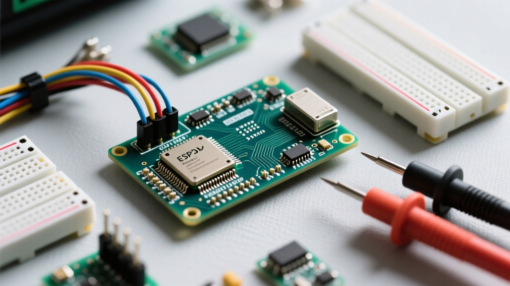
One of the most critical, yet poorly documented, aspects of modern ESP32 pinouts is the concept of strapping pins. These are specific GPIO pins that the internal bootloader reads during the very first milliseconds of power-on to determine the chip's boot mode and flash voltage.
The primary ESP32 strapping pins include GPIO0, GPIO2, GPIO12, and GPIO15. If you wire a sensor or a pull-up resistor to GPIO12 that pulls the pin HIGH during boot, the ESP32 will incorrectly configure its internal flash memory interface to 1.8V instead of the standard 3.3V. Because almost all third-party DevKits use 3.3V SPI flash chips, this strapping pin misconfiguration will result in a bootloop and a flash read err, 1000 panic in the serial monitor. When designing custom PCBs or complex breadboard circuits, always cross-reference your wiring against the silicon manufacturer's strapping pin requirements to ensure these pins are left floating or pulled to their safe default states during reset.
Comparative Analysis: ATmega328P vs. ESP32 vs. RP2040
To illustrate how drastically GPIO pinouts and their underlying hardware capabilities differ across architectures, review the comparison table below. This data is essential for selecting the right MCU for your specific I/O requirements.
| Feature | Arduino Uno R3 (ATmega328P) | ESP32 DevKitC V4 | Raspberry Pi Pico (RP2040) |
|---|---|---|---|
| Logic Level | 5V | 3.3V | 3.3V |
| Total Usable GPIOs | 14 Digital + 6 Analog | ~30 (varies by board) | 26 Multi-function |
| Max Continuous Current/Pin | 20 mA | ~12-20 mA | 12 mA |
| ADC Resolution | 10-bit (6 channels) | 12-bit (15 channels) | 12-bit (4 channels) |
| Default I2C Pins | SDA: A4 / SCL: A5 | SDA: GPIO21 / SCL: GPIO22 | SDA: GPIO4 / SCL: GPIO5 |
| Hardware PWM Channels | 6 | 16 (LED PWM) | 16 (8 slices) |
Multiplexing and Alternate Functions Explained
Modern MCU pinouts rarely dedicate a single physical pin to a single function. Instead, they utilize multiplexing and alternate functions via internal pin control registers. A single GPIO pin on the RP2040, for instance, can be configured in software as a standard digital I/O, a hardware PWM output, an I2C data line, an SPI clock, or a PIO (Programmable I/O) state machine input.
When reading a comprehensive pinout diagram, you will often see a grid or color-coded matrix indicating these alternate functions. For example, while GPIO18 and GPIO19 on the ESP32 are commonly used for the VSPI bus (MISO and CLK), they can also be remapped to route internal DAC or touch sensor signals. Understanding multiplexing allows you to rescue a PCB design when you realize you have routed a trace to a pin that lacks the specific hardware peripheral (like a dedicated UART TX line) you actually needed.
Practical Troubleshooting: When Your GPIO Pinout Fails
Even with a perfect wiring diagram, hardware bugs occur. Here are the most common failure modes related to GPIO configuration and how to debug them:
- Floating Pins and Ghost Readings: If a GPIO configured as an INPUT is not connected to a definitive HIGH or LOW voltage, it will act as an antenna, picking up electromagnetic interference. This results in erratic
digitalRead()values. Always enable internal pull-up or pull-down resistors in your code (e.g.,pinMode(pin, INPUT_PULLUP)) or use external 10kΩ resistors. - Backfeeding Through Protection Diodes: If you power down your microcontroller but leave a 5V sensor connected to a 3.3V GPIO pin, current will flow backward through the MCU's internal ESD protection diodes, effectively powering the chip in an undefined brownout state. Use series resistors or dedicated level shifters with high-impedance states to prevent this.
- ADC Non-Linearity at the Rails: When using analog GPIO pins, note that most MCUs cannot read accurately all the way to 0V or VCC. The ESP32 ADC is notoriously non-linear below 0.1V and above 3.1V. If your sensor outputs 3.3V, the ESP32 pinout might read it as 4095, but a 3.2V signal might also read as 4095. Design voltage dividers to keep analog signals in the 0.2V to 2.8V sweet spot.
Always consult the official silicon datasheet, not just the third-party development board silkscreen, when designing permanent PCBs or dealing with high-speed communication protocols.
For authoritative electrical specifications and exact pin multiplexing matrices, always refer to the primary silicon datasheets: