
The Limits of Sequential Processing: Why Migrate?
For years, the Arduino ecosystem has been the undisputed king of rapid prototyping. However, as maker projects evolve into industrial-grade edge devices, the sequential nature of standard microcontrollers (MCUs) becomes a hard bottleneck. When your Arduino sketch is bogged down by interrupt latency, software-based PWM jitter, or the inability to sample multiple high-speed ADCs simultaneously, it is time to consider a hardware migration.
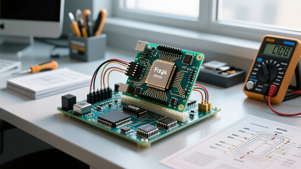
Integrating an FPGA with Arduino creates a hybrid architecture: the MCU handles high-level control, networking, and user interfaces, while the FPGA executes deterministic, parallel hardware logic. This guide details the exact migration path, hardware selection, and interface protocols required to upgrade your project in 2026.
Decision Matrix: Do You Actually Need an FPGA?
Before rewriting your C++ firmware into Verilog or VHDL, evaluate your project against this migration matrix. FPGAs introduce significant complexity; they should only be deployed when software optimization fails.
| System Requirement | MCU Only (e.g., Portenta H7 / Teensy 4.1) | Hybrid (FPGA with Arduino) |
|---|---|---|
| Parallel I/O Processing | Sequential polling (High latency) | True parallel execution (Zero latency) |
| Digital Signal Processing | Software DSP (Consumes CPU cycles) | Hardware MAC units & Pipelining |
| Deterministic Timing | Interrupt jitter (Microseconds) | Clock-cycle exact (Nanoseconds) |
| Development Time | Hours to Days | Weeks (RTL design + Testbenches) |
| BOM Cost (2026 Estimates) | $25 - $115 | $60 - $250+ |
The 2026 Hardware Stack: Moving Past Legacy Boards
In the late 2010s, the Arduino MKR Vidor 4000 was the go-to board for FPGA integration, pairing a SAMD21 with an Intel Cyclone 10LP. However, by 2026, the Vidor is largely discontinued and unsupported. Modern migration requires a modular, high-performance stack.
The Recommended Upgrade Path
- The MCU: Arduino Portenta H7 (~$115). Featuring a dual-core STM32H747XI (Cortex-M7 at 480MHz and Cortex-M4 at 240MHz), it provides the raw throughput needed to feed data to an FPGA via high-speed SPI or QSPI.
- The FPGA: Sipeed Tang Nano 20K (~$28). Built on the Gowin GW2A-LV18QN88C8/I7 architecture, it offers 20,736 LUT4s, 1,008 Kbits of Block RAM, and a hard DDR3 controller. It is currently the most cost-effective entry point for serious RTL development.
Expert Insight: Do not attempt to bit-bang parallel buses between the Portenta and the FPGA using standard GPIO. The capacitance of long jumper wires will cause signal integrity failures above 10 MHz. Always use dedicated SPI hardware peripherals or level-shifted QSPI for the bridge.
Bridging the Architecture: The SPI Interface
The most reliable method for linking an FPGA with Arduino is the Serial Peripheral Interface (SPI). While I2C is too slow for data streaming and UART lacks synchronous clocking, SPI provides a robust, full-duplex byte stream.
Wiring and Signal Integrity
When routing SPI lines between the Portenta H7 (3.3V logic) and the Tang Nano 20K (3.3V/1.8V bank dependent), you must mitigate ground bounce and reflections.
- Series Termination: Solder 33Ω series resistors on the MOSI, MISO, and SCK lines as close to the source pin as possible. This matches the trace impedance and eliminates ringing.
- Grounding: Use at least two ground wires between the MCU and FPGA breakout boards to minimize the ground loop inductance.
- Level Shifting: If your FPGA I/O bank is configured for 1.8V (common for high-performance Gowin banks), use a dedicated bidirectional level shifter like the TXS0108E, though be aware of its propagation delay limiting SPI clocks to ~20 MHz.
Firmware Configuration (Arduino C++)
On the Arduino side, configure the SPI bus using explicit transaction settings to avoid phase mismatches. FPGAs typically default to SPI Mode 0 (CPOL=0, CPHA=0).
SPI.beginTransaction(SPISettings(14000000, MSBFIRST, SPI_MODE0));
Running the Portenta H7 SPI bus at 14 MHz is the practical sweet spot. Pushing it to the theoretical 50+ MHz maximum often results in corrupted payloads due to breadboard parasitics and FPGA input register setup-time violations.
Logic Partitioning: What Goes Where?
A common mistake during migration is attempting to port the entire Arduino sketch into Verilog. The golden rule of hybrid design is partitioning by domain.
Keep in the Arduino MCU (C/C++)
- Wi-Fi/Bluetooth stack management and MQTT publishing.
- SD card file system operations (FAT32/exFAT).
- Display rendering (LVGL) and user input debouncing.
- High-level PID tuning parameters and configuration profiles.
Migrate to the FPGA (Verilog/VHDL)
- Hardware-in-the-Loop (HIL) PWM: Generating sub-microsecond dead-time complementary PWM signals for motor control.
- Digital Filtering: Implementing FIR/IIR filters on raw ADC data before it ever reaches the MCU's RAM.
- State Machines: High-speed quadrature encoder decoding and velocity calculation.
Critical Failure Modes and Edge Cases
Migrating to an FPGA introduces hardware-level failure modes that do not exist in sequential software. Pay strict attention to the following edge cases.
1. Clock Domain Crossing (CDC)
Your SPI bridge operates on the Arduino's SCK, but your internal FPGA logic likely runs on a separate 27MHz or 50MHz oscillator. Passing data between these domains without synchronization will cause metastability, leading to random, unrepeatable system crashes. According to the Intel FPGA Clock Domain Crossing Guidelines, you must implement dual-flop synchronizers or asynchronous FIFOs for any signal crossing clock boundaries. Never route an SPI-derived clock directly to internal flip-flops without proper CDC handling.
2. SPI Payload Framing Errors
Unlike software UART, SPI has no inherent start/stop bits or packet framing. If the Arduino resets or the Chip Select (CS) line glitches, the FPGA's SPI shift register will permanently misalign by one bit. The Fix: Implement a hardware state machine in the FPGA that monitors the CS line. On the rising edge of CS, force the shift register to clear and reset the byte-counter to zero. Always use a 10kΩ pull-up resistor on the CS line to prevent floating states during MCU boot-up.
3. Resource Exhaustion and Routing Congestion
Beginners often write highly unoptimized Verilog that consumes excessive Look-Up Tables (LUTs). Before finalizing your migration, consult the AMD UltraFast Design Methodology (applicable conceptually across all FPGA vendors) regarding pipelining. Inserting pipeline registers between complex combinatorial logic blocks reduces routing congestion and allows the Gowin or Xilinx synthesis tools to achieve higher Fmax (maximum clock frequency) without timing violations.
Summary of the Migration Workflow
Upgrading to a hybrid FPGA with Arduino architecture is not a simple plug-and-play endeavor; it is a fundamental shift in how you conceptualize time and data flow. By selecting a modern stack like the Portenta H7 and Tang Nano 20K, enforcing strict SPI signal integrity, and rigorously partitioning your logic domains, you can break free from the limits of sequential processing and build truly deterministic, industrial-grade edge devices.