
The Genesis of the RP2040 in the Arduino Ecosystem
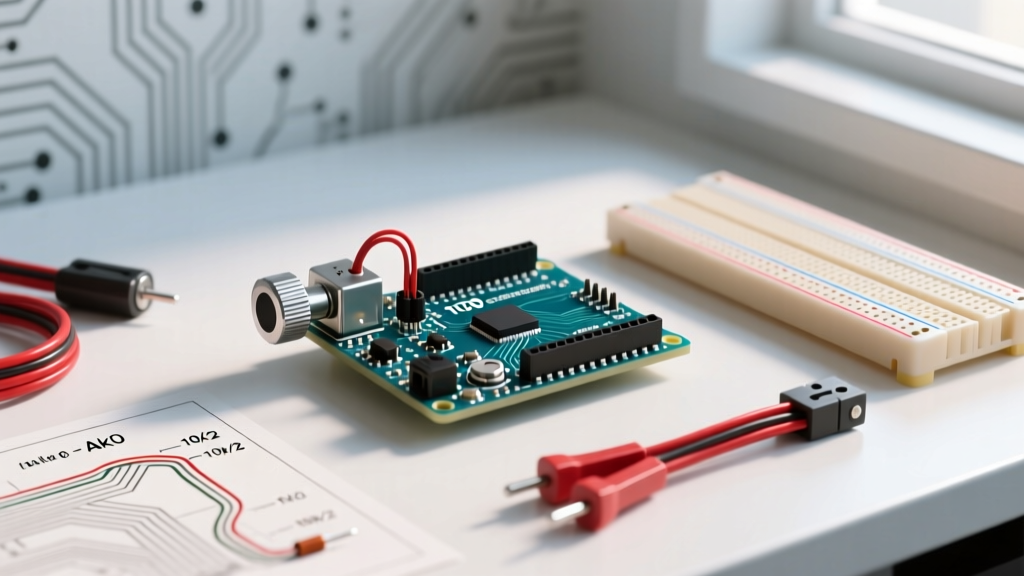
When the RP2040 silicon was first introduced, it fundamentally disrupted the microcontroller market by offering high performance, dual-core processing, and a unique peripheral architecture at a remarkably low price point. While originally designed by the Raspberry Pi Foundation, the chip quickly became a cornerstone of the broader maker ecosystem. Today, when engineers and hobbyists refer to the Arduino RP2040, they are typically discussing either the official Arduino Nano RP2040 Connect or the widespread integration of the RP2040 chip into the Arduino IDE via community-driven board packages.
As of 2026, the RP2040 has matured from a novel release into an industry staple. Its seamless integration with the Arduino IDE—largely championed by the arduino-pico community core—has allowed developers to leverage familiar C++ sketches while unlocking advanced hardware features that older 8-bit AVR microcontrollers simply cannot handle.
Inside the Silicon: Dual-Core ARM Cortex-M0+ Architecture
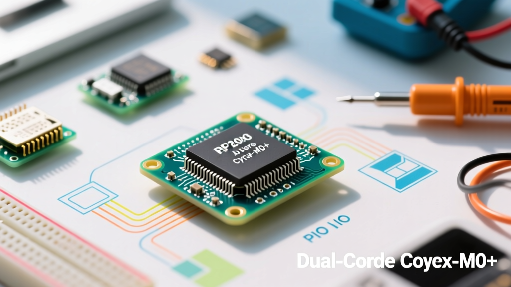
At the heart of the RP2040 is a dual-core ARM Cortex-M0+ processor running at a default clock speed of 133 MHz. Unlike older single-core microcontrollers where handling high-speed sensor polling and wireless communication simultaneously causes blocking delays, the RP2040 allows true parallel task execution. Core 0 can manage the primary application logic and USB stack, while Core 1 handles computationally heavy DSP (Digital Signal Processing) tasks or background peripheral management.
The Memory Matrix: SRAM and XIP Flash
One of the most defining architectural choices of the RP2040 is its memory layout. The chip contains exactly 264 KB of internal SRAM, divided into four striped banks. This striping allows the two cores and the DMA (Direct Memory Access) controller to access memory simultaneously with minimal bus contention. Furthermore, the RP2040 features no internal flash memory. Instead, it relies on external QSPI flash chips (typically ranging from 2 MB to 16 MB on commercial boards). Code execution happens via a dedicated XIP (eXecute In Place) cache, which transparently fetches instructions from the external flash, making the system behave as though the flash is internal memory.
The Secret Weapon: Programmable I/O (PIO) State Machines
If there is one feature that elevates the RP2040 above competing microcontrollers in its price class, it is the Programmable I/O (PIO) subsystem. Detailed extensively in the official RP2040 hardware documentation, the PIO block consists of four independent state machines, each equipped with its own instruction set and FIFO (First-In-First-Out) buffers.
Expert Insight: The PIO blocks are completely independent of the main Cortex-M0+ cores. A single PIO state machine can generate precise hardware-level timing signals—such as the strict 800 KHz pulse train required by WS2812B addressable LEDs—using zero CPU cycles. This leaves both main cores entirely free to handle complex application logic, network stacks, or user interfaces.
Each PIO instruction is 32 bits wide and executes in a deterministic number of clock cycles. This allows developers to create custom hardware interfaces on the fly. Need a quadrature encoder interface? A custom UART baud rate? A high-speed I2S audio bus? You can write a few lines of PIO assembly to create these interfaces in software, mapping them to almost any GPIO pin on the chip.
Hardware Comparison: Arduino Nano RP2040 Connect vs. Pico
Choosing the right physical board for your RP2040 project depends heavily on your requirements for wireless connectivity, form factor, and budget. Below is a structural comparison of the most popular RP2040 boards used within the Arduino ecosystem in 2026.
| Feature | Arduino Nano RP2040 Connect | Raspberry Pi Pico | Raspberry Pi Pico W |
|---|---|---|---|
| Core MCU | RP2040 (Dual Cortex-M0+) | RP2040 (Dual Cortex-M0+) | RP2040 (Dual Cortex-M0+) |
| Wireless | Wi-Fi & BLE (u-blox NINA-W102) | None | Wi-Fi & BLE (Infineon CYW43439) |
| Onboard Sensors | 6-Axis IMU, Microphone, Crypto Chip | Temperature Sensor only | Temperature Sensor only |
| Form Factor | Arduino Nano (Breadboard friendly) | Pico (Stamp module) | Pico (Stamp module) |
| Approx. Price (2026) | $24.00 - $27.00 | $4.00 | $6.00 |
The Arduino Nano RP2040 Connect documentation highlights its integrated u-blox NINA-W102 module, which provides robust Wi-Fi and Bluetooth Low Energy capabilities alongside an onboard ECC608 crypto chip for secure IoT provisioning. However, for cost-sensitive projects where wireless is handled externally (or not needed), the baseline $4 Pico remains unbeatable.
Common Pitfalls and Edge Cases in RP2040 Development
While the Arduino IDE abstracts much of the hardware complexity, working directly with the RP2040 silicon introduces specific edge cases that catch many developers off guard. Understanding these failure modes is critical for designing robust embedded systems.
1. External Flash Wear and Tear
Because the RP2040 executes code from external QSPI flash, some developers attempt to use a portion of this flash for non-volatile data storage (emulating EEPROM). Do not do this without a robust wear-leveling algorithm. Standard SPI flash chips are typically rated for 100,000 erase cycles. If your sketch writes sensor logs to the same flash sector every few seconds, you will brick the board's flash memory in a matter of days. Always use dedicated external I2C/SPI EEPROM chips for high-frequency logging, or utilize the LittleFS library which includes basic wear-leveling.
2. The I2C Pull-Up Misconception
The RP2040's GPIO pins do feature internal pull-up resistors, but they are exceptionally weak (typically around 50kΩ to 60kΩ). The I2C specification requires much stronger pull-ups to achieve proper signal rise times, especially at 400 KHz (Fast Mode). If you connect an I2C sensor without external 4.7kΩ or 2.2kΩ pull-up resistors on the SDA and SCL lines, your bus will experience intermittent data corruption or fail to enumerate entirely.
3. ADC Noise and the Floating Input Issue
The RP2040 features a 12-bit ADC with four accessible channels (GPIO26, GPIO27, GPIO28, and an internal temperature sensor). However, the ADC is notoriously noisy compared to dedicated analog microcontrollers. To get clean readings:
- Implement hardware averaging in your code (take 16 to 64 samples and average them).
- Ensure all unused ADC-capable GPIO pins are configured as digital outputs or tied to ground. Leaving them floating introduces severe capacitive crosstalk into the active ADC channels.
- Power the ADC logic (ADC_VREF) from a clean, dedicated 3.3V LDO rather than the noisy USB VBUS line.
4. Recovering from a Bricked USB Stack
If you upload a sketch that crashes the USB stack or disables the GPIO pins responsible for USB communication, the board will disappear from your computer's device manager. Fortunately, the RP2040 features a hardware-level fallback in its bootrom. By holding down the BOOTSEL button on the board while plugging it into USB, the chip bypasses the external flash entirely and boots into an internal USB mass-storage mode. You can then drag and drop a new compiled .uf2 file directly onto the drive to recover the board.
Frequently Asked Questions (FAQ)
Can I use standard Arduino libraries with the RP2040?
Yes. The vast majority of standard Arduino libraries (like Wire, SPI, and Servo) are fully supported. However, libraries that rely on direct AVR register manipulation (such as older versions of FastLED or specific hardware-timed PWM libraries) will fail to compile. You must use RP2040-compatible forks or rely on the board's native PIO for high-speed signal generation.
Is the RP2040 suitable for battery-powered IoT projects?
While the Cortex-M0+ cores are highly power-efficient, the RP2040 lacks a dedicated low-power 'deep sleep' mode that completely shuts down the core while retaining RAM state via a secondary RTC (Real-Time Clock). It does have a 'Dormant' mode, but waking from it requires external GPIO interrupts. For ultra-low-power applications requiring timed wake-ups, microcontrollers like the ESP32-C3 or nRF52840 are generally better suited.
How far can I overclock the RP2040?
The default clock is 133 MHz, but the silicon is highly resilient. Many developers routinely overclock the RP2040 to 250 MHz or even 275 MHz without active cooling, provided the flash chip can handle the increased QSPI bus speed. Pushing past 300 MHz usually requires a dedicated heatsink and careful tuning of the core voltage (VREG), which risks long-term silicon degradation.