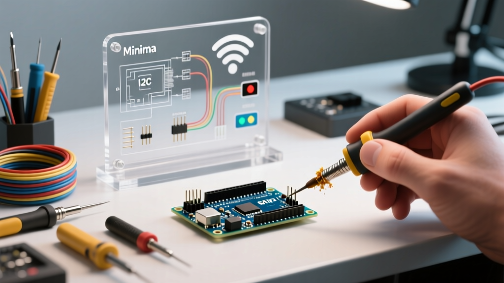

The Evolution of the Board: Why the R4 Pinout Matters
For over a decade, makers relied on the ATmega328P-based Uno R3, memorizing its 5V logic and limited peripheral set. However, as of 2026, the Arduino Uno R4 Minima and Uno R4 WiFi have completely replaced the R3 in professional prototyping and institutional kits. Priced around $22 and $28 respectively, these boards are powered by the 32-bit Renesas RA4M1 ARM Cortex-M4 microcontroller. Understanding the modern Arduino pinout diagram is no longer just about finding ground and 5V; it requires navigating 3.3V logic tolerances, multiplexed communication buses, and advanced analog peripherals like a 12-bit DAC and an internal operational amplifier.
Misinterpreting the R4 pinout diagram is the leading cause of fried GPIO pins and silent I2C failures in modern maker projects. This configuration guide breaks down the exact electrical characteristics, hidden routing paths, and peripheral limitations you must know before wiring your next circuit.
Core Power & Logic Level Matrix
The most critical shift in the modern Arduino pinout diagram is the transition from 5V to 3.3V logic. While the board still features a 5V power rail (derived from the USB input or the VIN barrel jack), the RA4M1 microcontroller operates natively at 3.3V. Feeding a 5V digital signal directly into a standard GPIO pin will destroy the silicon.
| Feature | Uno R3 (ATmega328P) | Uno R4 Minima (RA4M1) | Uno R4 WiFi (RA4M1 + ESP32-S3) |
|---|---|---|---|
| Native Logic Level | 5.0V | 3.3V | 3.3V |
| Max GPIO Current (Per Pin) | 20 mA (Recommended) | 8 mA (Recommended) | 8 mA (Recommended) |
| Total 5V Rail Capacity | ~500 mA (USB dependent) | 500 mA (via VUSB jumper) | 500 mA (via VUSB jumper) |
| Hardware I2C Pins | A4 (SDA), A5 (SCL) | A4 (SDA), A5 (SCL) | A4 (SDA), A5 (SCL) |
| DAC Resolution | None (Requires PWM) | 12-bit (Pin A0) | 12-bit (Pin A0) |
Configuration Pro-Tip: To pull the full 500mA from the USB-C port on the Uno R4, you must bridge the VUSB jumper pad located near the USB port. By default, this pad is open to protect downstream USB hubs from overcurrent events. If your pinout diagram shows a 5V sensor drawing 300mA, close this solder jumper first.
Advanced Peripherals: DAC, OpAmp, and CAN Bus Routing
The standard Arduino pinout diagram often glosses over the RA4M1's advanced analog features. To leverage these, you must look at the detailed technical schematics provided in the Renesas RA4M1 official documentation.
Configuring the 12-Bit DAC (Pin A0)
Unlike the R3, which faked analog output using PWM, the Uno R4 features a true 12-bit Digital-to-Analog Converter mapped to pin A0. However, there is a hardware caveat: the native output swing of the DAC is limited to approximately 0V to 2.3V. If your project requires a 0-3.3V or 0-5V analog control signal (e.g., driving a 0-10V industrial motor controller via an op-amp), you cannot wire A0 directly. You must route A0 through the internal OpAmp or an external rail-to-rail amplifier circuit.
The Internal OpAmp (Pin A1)
Pin A1 is internally wired to a non-inverting operational amplifier. This is incredibly useful for buffering high-impedance sensors (like piezoelectric knock sensors or raw thermocouple amplifiers) without needing an external LM358 chip. To configure this, you must initialize the OpAmp via the Arduino IDE before reading the analog value:
#include <OpAmp.h>
void setup() {
  OpAmp.begin(OpAmp.GAIN_1X);
}
CAN Bus: The Hidden Phantom Pins
Many makers look at the Uno R4 pinout diagram searching for CAN_H and CAN_L. The RA4M1 natively supports CAN 2.0B, but the Uno R4 PCB does not include a CAN transceiver. To configure a CAN network, you must wire an external transceiver (like the TJA1050 or MCP2551, costing around $1.50) to the designated CAN TX and RX pins mapped on the digital header. Failing to use a transceiver and wiring the MCU pins directly to a CAN bus will result in immediate communication failure and potential bus shorting.
Navigating the Uno R4 WiFi ESP32-S3 Pinout Overlays
The Uno R4 WiFi hardware documentation reveals a dual-processor architecture. The primary RA4M1 handles your standard sketch and GPIO, while an ESP32-S3 module handles WiFi, Bluetooth, and the 12x8 LED matrix.
When reading the pinout diagram for the WiFi model, note that the ESP32-S3 is connected to the RA4M1 via a dedicated hardware UART (Serial1). If your project requires using Serial1 for an external GPS module or RS485 transceiver, you will conflict with the internal WiFi bridge. For 2026 IoT projects, it is highly recommended to use SoftwareSerial on alternative digital pins (e.g., D10/D11) for secondary peripherals, leaving the hardware UART exclusively for the ESP32-S3 bridge.
Step-by-Step Mixed-Voltage Sensor Configuration
A common scenario is wiring a 3.3V I2C environmental sensor (like the BME280) alongside a 5V electromechanical relay. Here is how to configure your wiring using the R4 pinout diagram safely:
- Power Routing: Connect the BME280 VCC to the 3.3V pin on the R4 header. Connect the Relay Module VCC to the 5V pin (ensure the VUSB jumper is closed).
- Grounding: Tie all GND pins together. The R4 features multiple GND pins on the digital and power headers; use the one closest to your signal wires to minimize ground loop noise.
- I2C Level Shifting: Although the R4's I2C pins (A4/A5) are 3.3V, many cheap BME280 breakout boards have 10k pull-up resistors tied to 5V on their PCB. To prevent 5V backfeeding into the RA4M1's A4/A5 pins, wire a BSS138 bidirectional logic level shifter between the R4 and the sensor.
- Relay Control: Wire the Relay IN pin to Digital Pin 8 (D8). Because the R4 outputs 3.3V logic, ensure your relay module is 'low-level trigger' or explicitly rated for 3.3V activation. Standard 5V high-level trigger relays will fail to switch with the R4's 3.3V GPIO output.
Common Pinout Misconfigurations & Troubleshooting
- I2C Scanner Fails on A4/A5: The RA4M1 internal pull-up resistors are weaker than the ATmega328P. If your I2C device lacks onboard pull-ups, the bus will float. Solder external 4.7kΩ pull-up resistors from A4 and A5 to the 3.3V rail.
- Analog Read Noise on A2/A3: The Uno R4 WiFi features a switching buck converter to step down 5V to 3.3V for the ESP32-S3. This introduces high-frequency switching noise into the 3.3V rail, which can corrupt sensitive analog readings on A2 and A3. Fix: Use a 100nF ceramic capacitor directly across your analog sensor's VCC and GND pins, or use the internal oversampling features in the Arduino IDE.
- Serial Monitor Garbage Output: The native USB port on the R4 is handled directly by the RA4M1's USB peripheral, not a secondary 16U2 chip like the R3. If you see garbage text, ensure your IDE baud rate matches your sketch exactly; the R4 does not auto-negotiate virtual COM port baud rates the same way the R3 did.
Frequently Asked Questions
Can I use 5V shields on the Uno R4?
Mechanically, yes. Electrically, it depends. Shields that only draw power from the 5V rail and use SPI (which is often 5V tolerant on shift registers) will work. However, shields that send 5V logic signals back into the R4's digital pins (like older motor shields without optocouplers) will damage the RA4M1. Always cross-reference the shield's schematic with the R4 pinout diagram.
Where is the SPI bus located on the R4 pinout?
Just like the R3, the primary hardware SPI bus is mapped to Digital Pins 11 (MOSI), 12 (MISO), and 13 (SCK), with Pin 10 typically used as Chip Select (CS). These pins are also duplicated on the 2x3 ICSP header, which remains fully 3.3V logic on the R4.