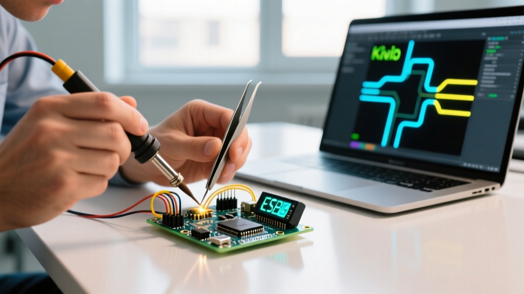

The Evolution from Breadboard to Custom PCB
Transitioning a microcontroller project from a messy breadboard to a manufactured Printed Circuit Board (PCB) is a major milestone for any maker. While breadboards are excellent for prototyping, they introduce parasitic capacitance, loose connections, and severe limitations for high-frequency or high-current applications. To bridge this gap, you need a reliable Arduino circuit diagram maker—a software tool capable of schematic capture, electrical rule checking, and physical PCB layout.
In 2026, the ecosystem for PCB design has matured significantly. Cloud-based tools offer instant component library syncing, while open-source desktop applications rival enterprise-grade suites that cost thousands of dollars. This tutorial will guide you through selecting the right software and executing a professional-grade PCB design for a custom Arduino-compatible board using the industry-standard, open-source tool: KiCad.
Comparing the Best Arduino Circuit Diagram Maker Tools
Before routing a single trace, you must choose the right environment. The term 'circuit diagram maker' encompasses everything from simple educational simulators to full-scale CAD suites. Below is a comparison of the top tools used by the maker and engineering communities today.
| Tool | Pricing (2026) | Learning Curve | Best Use Case |
|---|---|---|---|
| KiCad (v8/v9) | Free / Open Source | Moderate to High | Professional custom PCBs, complex multi-layer designs. |
| EasyEDA Pro | Free (Standard) / $99/yr | Low to Moderate | Rapid prototyping with direct LCSC/JLCPCB integration. |
| Fritzing | ~$8.00 One-time | Very Low | Beginners, simple single-layer shields, visual documentation. |
| Tinkercad Circuits | Free | Very Low | Code simulation and basic wiring; no PCB export. |
For this tutorial, we will use KiCad. It provides unlimited board size, no layer restrictions, and outputs standard Gerber files accepted by every fabrication house globally. According to the KiCad Official Documentation, the software supports push-and-shove routing and 3D viewer integration, making it the undisputed champion for serious open-source hardware development.
Step-by-Step: Designing an Arduino-Compatible Board
We will design a standalone board centered around the ATmega328P-AU (TQFP-32 surface mount package), which is significantly more compact and reliable than the through-hole DIP-28 version used on breadboards.
Phase 1: Schematic Capture and Component Selection
The schematic is the logical representation of your circuit. Open KiCad and create a new project. Press 'E' to open the schematic editor.
- Microcontroller Placement: Search for
ATmega328P-AU. Place it in the center of your workspace. - Clock Circuit: The ATmega328P requires an external crystal for 16MHz operation. Place a 16MHz HC49/S or SMD 3225 crystal. Connect it to pins XTAL1 (PB6) and XTAL2 (PB7). Crucial Detail: Add two 22pF load capacitors to ground. You must specify the dielectric as C0G/NP0, not X7R. X7R ceramics exhibit piezoelectric effects and microphonics that can cause clock jitter and erratic MCU behavior.
- Decoupling Capacitors: Place a 100nF (0.1µF) X7R ceramic capacitor on every VCC and AVCC pin. These must be placed logically near the pins to filter high-frequency switching noise.
- Reset Circuit: Add a 10kΩ pull-up resistor to the RESET pin (PC6). To enable auto-reset via a USB-to-Serial adapter (like the FTDI FT232RL), place a 100nF capacitor in series with the DTR line leading to the RESET pin.
- ISP Header: Add a 2x3 pin header (2.54mm pitch) wired to the SPI pins (MOSI, MISO, SCK), RESET, VCC, and GND for bootloader flashing.
Phase 2: Footprint Assignment and ERC
Once the logical schematic is complete, you must map each symbol to a physical PCB footprint. Press 'C' on a component to open the footprint assignment tool.
- Map the ATmega328P-AU to
Package_QFP:TQFP-32_7x7mm_P0.8mm. - Map the 100nF capacitors to
Capacitor_SMD:C_0603_1608Metric(0603 imperial size is the sweet spot for hand soldering and automated assembly). - Run the Electrical Rules Check (ERC). This tool flags unconnected pins, power shorts, and missing power flags. Resolve all errors before proceeding.
Phase 3: PCB Layout, Routing, and Ground Planes
Press 'F8' to update the PCB from the schematic. You will see a rat's nest of thin white lines indicating logical connections.
- Component Placement: Group components by function. Keep the crystal and its 22pF capacitors as close to the XTAL pins as physically possible—ideally within 3mm. Refer to the Texas Instruments PCB Layout Guidelines for high-speed signal isolation techniques.
- Trace Routing: Use the interactive router (X). Set your grid to 0.1mm. For standard digital signals (I/O, SPI, I2C), use a trace width of 0.254mm (10 mils). For power (5V) and ground lines, increase the width to 0.508mm (20 mils) or larger to reduce resistance and voltage drop.
- Vias: When transitioning between the top and bottom layers, use vias with a 0.3mm drill size and a 0.6mm annular pad. This complies with the standard capabilities of budget fab houses like JLCPCB and PCBWay.
- Ground Plane: Assign the bottom copper layer (B.Cu) entirely to the GND net. This creates a solid reference plane, drastically reducing electromagnetic interference (EMI) and providing a low-impedance return path for high-frequency signals.
Critical Failure Modes and Edge Cases
Even with a perfect schematic, physical layout errors can render an Arduino board unstable. Watch out for these common failure modes:
1. The Decoupling Capacitor Trap
Placing a decoupling capacitor on the same side of the board but routing it through long, looping traces defeats its purpose. The capacitor must have a direct, low-inductance path to the MCU's power and ground pins. Solution: Place the 0603 capacitor directly between the VCC pin and a via that drops immediately to the bottom ground plane.
2. USB Impedance Mismatches
If your design includes a native USB interface (e.g., using an ATmega32U4 instead of the 328P), the D+ and D- lines are high-speed differential pairs. They require a 90-ohm differential impedance. Solution: Use KiCad's built-in length-tuning and impedance calculator tools to route these traces parallel to each other, exactly 0.2mm apart, over a continuous ground plane.
3. Analog Reference Noise
The AREF pin is highly susceptible to digital switching noise. If you are reading analog sensors (like a potentiometer or NTC thermistor), never route AREF traces parallel to digital I/O lines. Use the Arduino Official Pin Mapping documentation to identify physical pin locations and keep analog routing isolated to one corner of the PCB.
Pro-Tip for Manufacturing: When ordering 2-layer FR4 boards in 2026, standard HASL (Hot Air Solder Leveling) finish is cheapest (~$2 for 5 boards). However, because the TQFP-32 package has a tight 0.8mm pin pitch, select ENIG (Electroless Nickel Immersion Gold) finish. It costs slightly more but provides a perfectly flat surface, preventing solder bridging during reflow or hand soldering.
Exporting Gerbers for Manufacturing
Once your Design Rule Check (DRC) passes with zero errors and zero unconnected items, it is time to export the manufacturing files.
- Go to File > Fabrication Outputs > Gerbers (.gbr).
- Select the standard coordinate format (4.6) and ensure all copper layers, silkscreen, solder mask, and edge cuts are checked.
- Generate the Drill Files (.drl) in the same directory.
- Zip the folder containing the .gbr and .drl files.
Upload this ZIP file to your preferred PCB fabrication service. Within 3 to 5 days, you will receive a batch of professional, custom-designed Arduino boards ready for component population. By mastering your Arduino circuit diagram maker of choice, you eliminate the limitations of off-the-shelf modules and unlock the true potential of embedded hardware design.