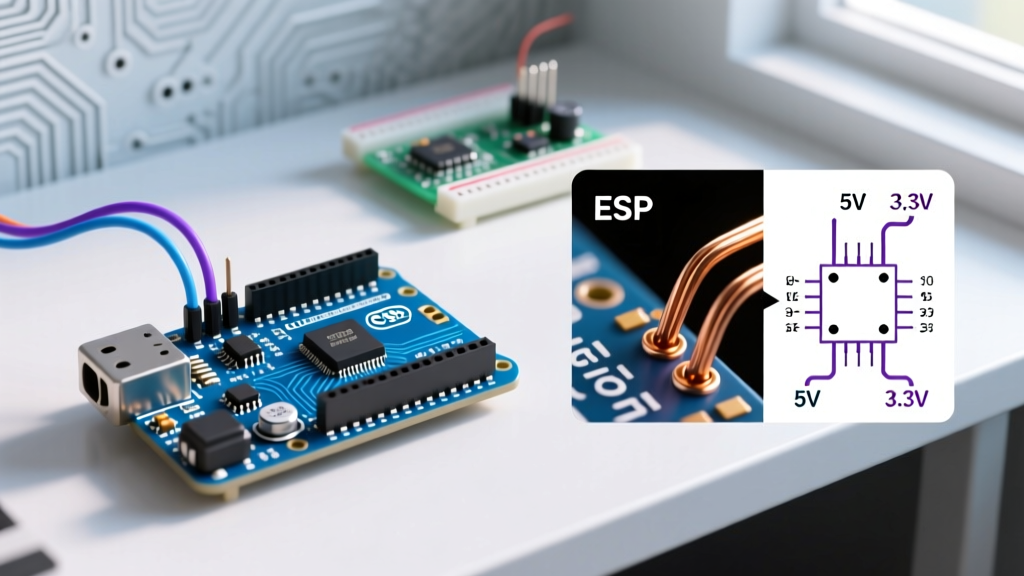

The Hidden Danger in Legacy Arduino Circuit Diagrams
When drafting an Arduino circuit diagram, the most common point of catastrophic failure isn't a misplaced wire or an undersized power supply—it is an unaddressed logic level mismatch. For over a decade, the maker community relied on the 5V logic of the ATmega328P found in the classic Uno R3 and Nano. However, the modern ecosystem has aggressively pivoted to 3.3V architectures. Boards like the Arduino Uno R4 WiFi (powered by the Renesas RA4M1) and the Arduino Nano ESP32 operate strictly at 3.3V on their GPIO pins.
If you take a legacy 5V schematic and map it directly to a modern 3.3V microcontroller without implementing proper translation, you risk backfeeding voltage rails, bricking I2C buses, and permanently damaging internal ESD protection diodes. This compatibility guide breaks down exactly how to adapt your schematics, select the right logic level shifters, and avoid the most common pinout traps in 2026.
Board-to-Board Pinout and Logic Translation Matrix
Before routing traces or placing components on a breadboard, you must understand the electrical characteristics of your target MCU. The table below compares the legacy standard with modern alternatives, highlighting critical differences in current sourcing and logic thresholds.
| Board Model | Core MCU | Logic Level | I2C Default Pins | SPI Default Pins | Max Continuous GPIO Current |
|---|---|---|---|---|---|
| Uno R3 | ATmega328P | 5.0V | A4 (SDA), A5 (SCL) | 11 (MOSI), 12 (MISO), 13 (SCK) | 20 mA (40 mA absolute max) |
| Uno R4 WiFi | Renesas RA4M1 | 3.3V | A4 (SDA), A5 (SCL) | 11 (MOSI), 12 (MISO), 13 (SCK) | 8 mA per pin |
| Nano ESP32 | ESP32-S3 | 3.3V | A4 (SDA), A5 (SCL) | D11 (MOSI), D12 (MISO), D13 (SCK) | 18 mA (40 mA peak) |
| Zero / MKR | SAMD21 | 3.3V | D20 (SDA), D21 (SCL) | D23 (MOSI), D22 (MISO), D24 (SCK) | 7 mA per pin |
Note: Always consult the official Arduino Uno R4 WiFi documentation or respective board schematics, as pin mappings for secondary SPI/I2C buses vary wildly between the RA4M1 and ESP32-S3 chips.
Translating Your Arduino Circuit Diagram Across Logic Families
Adapting a schematic from 5V to 3.3V requires more than just changing the power supply symbol. You must evaluate every peripheral connected to the MCU's digital pins. According to SparkFun's Logic Levels tutorial, a 3.3V device receiving a 5V signal will read the input as a logic HIGH, but the excess 1.7V must dissipate somewhere. In most MCUs, this excess voltage forces current through the internal clamp diodes to the VCC rail. If the current exceeds the diode's rating (typically 5mA to 10mA), the silicon permanently degrades, resulting in a shorted pin that reads constant HIGH or LOW.
The I2C Pull-Up Resistor Pitfall
I2C is an open-drain protocol that requires pull-up resistors. Most off-the-shelf sensor modules (like the BME280 or MPU6050) include 4.7kΩ pull-up resistors tied to the module's VCC pin.
- The 5V Scenario: If you power the module with 5V, the pull-ups go to 5V. The SDA/SCL lines idle at 5V. A 5V Uno R3 handles this perfectly.
- The 3.3V Failure Mode: If you power the module with 5V but connect the I2C lines to a 3.3V Nano ESP32, the 5V idle state will backfeed into the ESP32's 3.3V GPIO pins. Even if you power the module at 3.3V, using 4.7kΩ resistors on a 400kHz Fast-Mode I2C bus often results in signal rise-time failures due to bus capacitance.
The Fix: Remove the onboard module pull-ups (often by cutting a tiny trace or desoldering a 0603 resistor) and place external 2.2kΩ pull-up resistors directly to the 3.3V rail on your schematic. For bus capacitance over 200pF, drop to 1.0kΩ resistors to ensure the rise time stays under 300ns.
Selecting the Right Logic Level Shifter IC
When your Arduino circuit diagram must interface a 3.3V microcontroller with a 5V peripheral (like a legacy LCD1602 display, a 5V relay board, or WS2812B LED strips), you must insert a logic level translator. Choosing the wrong IC will corrupt high-speed data. Here is a comparison of the three most common shifters used in maker schematics:
1. BSS138 N-Channel MOSFET Shifter (Bidirectional)
The BSS138 is the gold standard for I2C and low-speed bidirectional signals. It utilizes a clever MOSFET gate configuration that safely translates voltages without backfeeding.
- Best For: I2C, 1-Wire, UART (up to 115200 baud).
- Cost: ~$1.50 to $2.50 for a 4-channel breakout board.
- Limitation: High gate capacitance limits bandwidth. Do not use for SPI clocks above 2 MHz.
2. TXS0108E (Bidirectional, Auto-Sensing)
Detailed extensively in the Texas Instruments TXS0108E datasheet, this IC uses internal one-shot edge accelerators to drive fast transitions. It is specifically designed for high-speed bidirectional buses.
- Best For: SPI (up to 50 MHz), SDIO, and high-speed UART.
- Cost: ~$3.50 to $5.00 for an 8-channel breakout.
- Limitation: It struggles with continuous DC signals or heavily capacitive loads. It is notorious for failing with I2C because the open-drain pull-down edges confuse the internal edge-detection circuitry.
3. CD4050B / 74LVC245 (Unidirectional)
If you only need to send signals from 3.3V to 5V (e.g., driving a 5V WS2812B LED strip data line or triggering a 5V relay), a simple unidirectional buffer powered by the 5V rail will accept 3.3V as a valid HIGH input (since 3.3V > 2.0V Vih threshold for standard CMOS).
- Best For: LED data lines, relay triggers, motor driver direction pins.
- Cost: ~$0.80 per IC.
Expert Schematic Tip: Never place decoupling capacitors on the signal lines of a logic level shifter. A common mistake in beginner Fritzing diagrams is adding a 100nF capacitor 'for noise filtering' on an I2C line. This will instantly destroy the I2C rise-time and cause bus lockups. Place your 100nF X7R ceramic capacitors strictly between the VCC and GND pins of the ICs.
Edge Cases: Input-Only Pins and Analog Mapping
When migrating an Arduino circuit diagram to the ESP32 family (including the Arduino Nano ESP32), you must account for the ADC and GPIO matrix limitations. Unlike the ATmega328P, where any analog pin (A0-A5) can be used as a digital I/O, the ESP32-S3 has strict hardware boundaries.
- GPIO 34 to 39 (on original ESP32) / Specific ADC2 Pins: Many pins on ESP32 variants are strictly input-only. They lack internal pull-up resistors and cannot drive an output HIGH or LOW. If your schematic routes a 5V signal through a voltage divider to one of these pins, ensure you are only reading analog data, never attempting to write to it.
- Strapping Pins (GPIO 0, 3, 46, 48): On the Nano ESP32, certain pins dictate the boot mode. If your circuit diagram ties GPIO 0 to GND via a pull-down resistor, the board will enter UART download mode on every reset and refuse to run your sketch. Always use pull-up resistors (10kΩ to 3.3V) on boot-critical pins if they must be connected to external buttons.
Step-by-Step: Finalizing Your Schematic for PCB Fabrication
Once your logic levels are mapped and shifters are selected, follow this checklist before exporting your Gerber files from KiCad or EasyEDA:
- Verify VCC Rails: Color-code your schematic nets. Red for 5V, Orange for 3.3V, Black for GND. Ensure no 5V net physically crosses into a 3.3V MCU pin without passing through a shifter or LDO regulator (like the AMS1117-3.3).
- Add Bulk Capacitance: Modern 3.3V Wi-Fi/BLE MCUs (like the RA4M1 and ESP32) experience massive current spikes (up to 350mA) during RF transmission. Your diagram must include at least one 10µF tantalum or low-ESR ceramic capacitor near the board's power input, alongside the standard 100nF decoupling caps.
- Check Trace Widths: A 5V relay drawing 70mA can use a standard 0.25mm (10 mil) trace. However, if your diagram includes a motor shield or high-power LED array, calculate your trace width using the IPC-2221 standard. A 1A continuous load requires roughly 0.5mm (20 mil) trace width on 1oz copper to prevent thermal throttling.
Frequently Asked Questions
Can I just use a voltage divider instead of a logic level shifter?
Yes, but only for low-speed, unidirectional signals. A simple resistor divider (e.g., 10kΩ series, 15kΩ to ground) will safely drop 5V down to ~3.0V for a 3.3V input. However, the parasitic capacitance of the resistors and the MCU pin will severely round off the square wave edges. This works fine for a simple push-button or a 9600-baud UART RX line, but it will cause data corruption on an SPI clock or I2C bus.
My Fritzing diagram works on a breadboard, but the PCB fails. Why?
Breadboards introduce significant parasitic capacitance and poor contact resistance, which ironically can sometimes dampen high-frequency ringing. When you move to a PCB, the clean, low-impedance traces can cause signal reflection on high-speed SPI/I2C lines if proper termination and layout practices aren't followed. Always add 33Ω to 47Ω series termination resistors directly at the source pin for SPI clock lines in your final schematic.