
Configuring Your Arduino Circuit Designer Environment
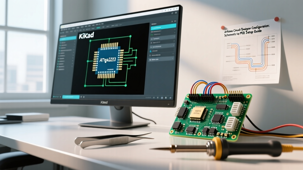
Transitioning from a solderless breadboard to a custom printed circuit board (PCB) requires a rigorous arduino circuit designer configuration. In 2026, the industry standard for independent makers, engineering students, and prototyping firms is a hybrid workflow: simulating logic in browser-based tools, then executing professional schematic capture and PCB layout in KiCad (versions 8.x and 9.x). This guide details the exact configuration steps required to design standalone Arduino boards and custom shields, ensuring your design passes manufacturing checks on the first run.
Unlike simple drag-and-drop wiring tools, a professional configuration demands strict adherence to Design Rule Checks (DRC), precise power delivery network (PDN) planning, and accurate footprint mapping. Below, we break down the exact parameters you need to configure your workspace for ATmega328P-based designs.
Step 1: Schematic Capture and Library Configuration
The foundation of any reliable Arduino circuit designer workflow is a verified component library. While the official Arduino ecosystem provides basic schematics, professional layouts require manufacturer-specific footprints.
Selecting the Right Microcontroller Variant
Before routing a single trace, you must configure your schematic symbols to match your physical component constraints:
- ATmega328P-PU (DIP-28): Ideal for through-hole prototyping and beginner soldering. Requires a larger board footprint (typically > 50x70mm for full shields).
- ATmega328P-AU (TQFP-32): The surface-mount standard for compact, production-ready designs. Requires a 4-layer PCB if you are routing high-density BGM or RF modules alongside the MCU.
- ATmega4809-AFR (TQFP-48): Used in modern Nano Every architectures. Requires careful pin-mapping configuration as it deviates from the legacy 328P pinout standards.
Crystal Oscillator Load Capacitor Math
A common failure mode in custom Arduino designs is an unstable clock signal due to incorrect load capacitor configuration. Do not blindly copy 22pF values from generic tutorials. Use the following formula to configure your C1 and C2 capacitors:
C = 2 * (C_L - C_stray)
If your 16MHz crystal specifies a load capacitance (C_L) of 18pF, and your PCB trace stray capacitance (C_stray) is approximately 5pF, your configured capacitors should be 2 * (18 - 5) = 26pF. Standardizing on 27pF C0G/NP0 dielectric capacitors is the safest configuration for 2026 manufacturing tolerances.
Step 2: Design Rule Check (DRC) Configuration for Maker Fabs
Your PCB layout software must be constrained by the physical limitations of your chosen fabrication house. Configuring your DRC parameters incorrectly will result in unmanufacturable boards or expensive engineering holds. Below is the recommended DRC matrix for the most popular maker-focused PCB manufacturers in 2026.
| Fabrication House | Min Trace / Spacing | Min Via Diameter / Hole | Standard 2-Layer Cost (5pcs) | Best Use Case |
|---|---|---|---|---|
| JLCPCB | 6mil / 6mil | 0.45mm / 0.3mm | $2.00 + Shipping | High-volume prototyping, standard shields |
| PCBWay | 6mil / 6mil | 0.45mm / 0.3mm | $5.00 + Shipping | Complex impedance control, flexible PCBs |
| OSH Park | 6mil / 6mil | 0.4mm / 0.2mm | $12.50 (per sq in) | Ultra-compact wearable Arduino nodes |
Note: Always verify the latest capabilities directly from the JLCPCB capabilities page or your chosen vendor before finalizing Gerber exports, as minimum via sizes frequently update with new laser drilling equipment.
Step 3: Power Delivery Network (PDN) Configuration
A robust Arduino circuit designer configuration isolates noisy digital switching from sensitive analog sensors. The power tree must be configured with specific decoupling and bulk capacitance.
Voltage Regulator Selection
For standalone boards powered by 7V-12V barrel jacks or LiPo batteries, configure your schematic with the AMS1117-5.0 linear regulator. While older designs used the L7805, the AMS1117 offers a lower dropout voltage (1.1V) and better thermal performance in SOT-223 packages.
Critical Configuration Rule: The AMS1117 requires a minimum of 10µF tantalum or 22µF low-ESR ceramic capacitors on both the input and output pins to prevent high-frequency oscillation. Placing a 0.1µF ceramic capacitor within 2mm of the microcontroller VCC pin is mandatory for high-speed ADC stability.
Analog vs. Digital Ground Planes
When configuring your copper pours in KiCad, do not merge AGND (Analog Ground) and DGND (Digital Ground) indiscriminately. Configure a single, unified ground plane, but use a 0-ohm resistor or a ferrite bead to bridge the analog and digital return paths near the main power supply entry point. This prevents digital return currents from flowing under the analog-to-digital converter (ADC) pins, which causes severe noise in analog sensor readings.
Step 4: Routing Constraints and Signal Integrity
Configuring your routing rules ensures signal integrity across the board. Modern Arduino designs frequently incorporate SPI displays, I2C sensor arrays, and USB-to-Serial ICs (like the CH340 or CP2102).
High-Speed Interface Routing
- USB D+ / D- Lines: Configure these as differential pairs with a 90-ohm impedance. Keep them strictly matched in length (within 5 mils) and avoid placing vias on these traces.
- SPI (SCK, MOSI, MISO): Route at 10mil to 12mil widths. Keep the SCK line as short as possible to minimize parasitic inductance, which can cause ringing at 8MHz+ clock speeds.
- I2C (SDA, SCL): Configure 4.7kΩ pull-up resistors physically adjacent to the master MCU. Route these lines away from the 16MHz crystal to prevent capacitive crosstalk.
Step 5: Generating Fabrication Outputs
The final phase of the Arduino circuit designer workflow is exporting the manufacturing files. In 2026, the legacy RS-274X format has been largely superseded by Gerber X2, which embeds stackup and file function metadata directly into the output.
- Run a full DRC and ERC (Electrical Rules Check). Resolve all unconnected net warnings.
- Generate Gerber X2 files for F.Cu, B.Cu, F.SilkS, B.SilkS, F.Mask, B.Mask, and Edge.Cuts.
- Export Excellon drill files (merged PTH and NPTH if your fab house supports it, or separate if required).
- Generate the BOM (Bill of Materials) and CPL (Component Placement List) in CSV format if you are utilizing automated PCBA (Printed Circuit Board Assembly) services.
Summary: Simulation vs. Physical Layout Tools
To maintain a streamlined workflow, it is vital to understand the boundaries of your software stack. Below is a comparison of how different tools fit into the modern Arduino design ecosystem.
| Tool Category | Software Example | Primary Function | Limitation |
|---|---|---|---|
| Logic Simulation | Tinkercad Circuits | Verifying code logic and basic wiring | Cannot model PCB parasitics or EMI |
| Schematic & Layout | KiCad 8/9 | Professional PCB routing and DRC | Steep learning curve for 3D modeling |
| Rapid Prototyping | Fritzing | Visual breadboard diagrams for tutorials | Poor autorouter, lacks advanced DRC |
By configuring KiCad as your primary physical layout engine and reserving browser-based simulators strictly for logic verification, you establish a professional-grade Arduino circuit designer pipeline. This methodology minimizes fabrication respins, reduces component waste, and ensures your custom microcontroller boards perform reliably in real-world environments.