
The Hidden Cost of Breadboard Prototyping
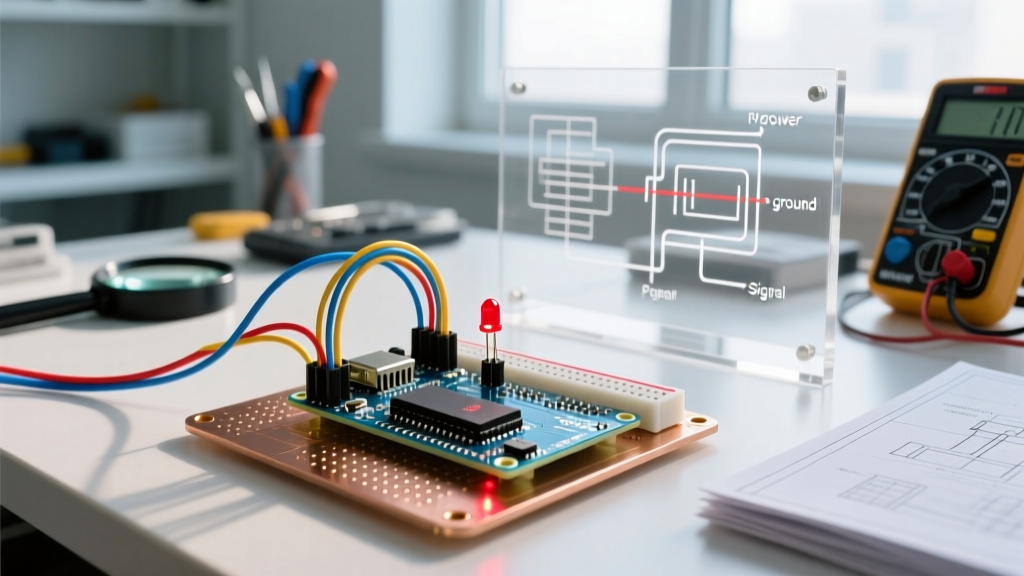
Every serious microcontroller project eventually hits the physical limits of a breadboard. Parasitic capacitance between adjacent traces, loose Dupont jumper wires, and the inability to test high-frequency RF modules like the ESP32-WROOM-32E reliably all force a transition to printed circuit boards. However, many makers stall at this phase, relying on outdated or overly simplistic tools that generate poor manufacturing files. Optimizing your Arduino CAD workflow is no longer just about drawing schematics; it is about establishing a seamless pipeline between Electronic Design Automation (ECAD) and Mechanical Design Automation (MCAD) to ensure your custom enclosures and PCBs fit together perfectly on the first revision.
In 2026, the gap between hobbyist and professional engineering tools has completely vanished. By adopting a structured CAD pipeline, you can reduce your prototyping iterations from three or four down to a single, highly reliable board spin. This guide details the exact workflow, toolchain, and design rules required to take your Arduino-based concepts from modular schematics to fully integrated mechanical assemblies.
Evaluating the Top Arduino CAD Ecosystems
Before optimizing your pipeline, you must select an ECAD tool that supports modern manufacturing constraints and 3D integration. The days of using Fritzing for professional-grade Gerber generation are over; modern design requires rigorous Design Rule Checking (DRC) and native 3D STEP file exports.
| Feature | KiCad 8/9 | Autodesk Fusion Electronics | EasyEDA Pro |
|---|---|---|---|
| Pricing (2026) | Free (Open Source) | Free for Hobbyists / $545/yr Commercial | Free Tier / $9.90/mo Pro |
| MCAD Integration | Native STEP Export (Push/Pull) | Unified ECAD/MCAD Environment | Basic 3D Viewer, No Native MCAD Sync |
| Library Management | Local & Git-based, Massive Community | Cloud-based, Unified Autodesk Library | Direct LCSC/JLCPCB Component Linking |
| Best For | Advanced Makers & Open Hardware | Complex Enclosure + PCB Co-design | Rapid 2-Layer Prototyping & Assembly |
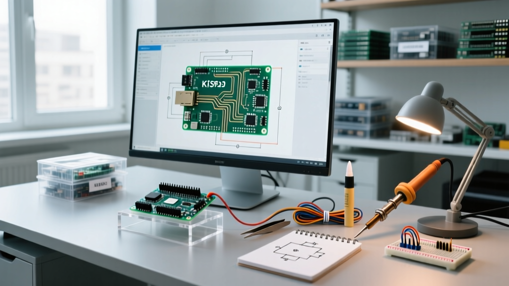
For makers focused on deep workflow optimization, KiCad remains the undisputed champion due to its unrestricted board sizes, hierarchical schematic support, and robust STEP file generation. However, if your primary bottleneck is designing complex, multi-part 3D-printed or CNC-machined enclosures around your Arduino PCB, Autodesk Fusion Electronics offers a unified environment where a change in the PCB outline instantly updates the mechanical constraints.
The Optimized 4-Stage Arduino CAD Pipeline
To eliminate bottlenecks, structure your design process into four distinct stages. This prevents the common mistake of simultaneously routing traces while debating component placement.
Stage 1: Modular Schematic Capture
Never redraw your core microcontroller circuit from scratch. The most efficient Arduino CAD workflow utilizes hierarchical sheets. Create a master repository of proven sub-circuits: an AMS1117-3.3 voltage regulator block, a USB-C receptacle block (using the GCT USB4085 footprint), and a standard ATmega328P-AU or ESP32-WROOM-32E break-out block.
When starting a new project, import these hierarchical blocks. This reduces schematic capture time by up to 70% and ensures that critical decoupling capacitors (e.g., 100nF X7R ceramics placed exactly 2mm from the MCU VCC pin) are never forgotten.
Stage 2: DRC-Driven PCB Routing
Before routing a single trace, configure your Design Rule Check (DRC) to match your chosen manufacturer's capabilities. For standard 2-layer boards manufactured by JLCPCB or PCBWay, set your net classes to the following baseline parameters:
- Signal Traces: 6 mil (0.15mm) width / 6 mil clearance.
- Power Traces (5V/3.3V): 12 mil to 20 mil width, depending on current draw (calculate using IPC-2221 standards).
- Vias: 0.3mm drill diameter / 0.45mm pad diameter.
- Annular Ring: Minimum 0.075mm.
Always route your high-speed differential pairs (like USB D+ and D-) first, matching their lengths within a 5-mil tolerance. Follow this with the RF antenna trace for ESP32 modules, ensuring a strict 50-ohm impedance profile and a complete keep-out zone on all copper layers beneath the antenna.
Stage 3: ECAD to MCAD Handoff
Once the board outline and critical component placement are finalized, export your PCB as a STEP (.step) file. Import this directly into your MCAD software (like Fusion 360 or SolidWorks). Do not wait until the PCB is fully routed to do this; verifying the mechanical fit of USB ports, mounting holes, and tall electrolytic capacitors early prevents catastrophic enclosure redesigns later.
Workflow Pro-Tip: Use M2 brass heat-set inserts (e.g., McMaster-Carr 94180A333) for your PCB mounting points. Design your PCB with 2.2mm unplated mounting holes, and design your 3D-printed enclosure with 3.2mm blind holes. This provides a vastly superior mechanical connection compared to self-tapping plastic screws, which strip after a single disassembly.
Stage 4: Design for Manufacturing (DFM) Review
Before generating Gerbers, run a final DFM check. Ensure all silkscreen text is at least 1.0mm tall with a 0.15mm line width to remain legible after printing. Verify that no silkscreen overlaps with exposed copper pads, which can cause solder to refuse to wet the pad during reflow. Finally, add a copper pour on both the F.Cu and B.Cu layers, tied to the GND net, to reduce electromagnetic interference (EMI) and improve thermal dissipation.
Common Failure Modes in Arduino Custom PCBs
Even with a perfect CAD workflow, specific edge cases routinely ruin first-time board spins. Watch for these specific failure modes:
- USB-C Shield Grounding Issues: Connecting the USB-C metal shield directly to the system ground can create ground loops and fail EMI testing. The optimized approach is to connect the shield to GND through a 1MΩ resistor in parallel with a 4.7nF Y-capacitor. This provides high-frequency noise shunting while preventing DC ground loops.
- ESP32 Antenna Keep-Out Violations: Placing a ground plane or signal trace directly beneath the ESP32 inverted-F antenna will detune the impedance, reducing wireless range by up to 80%. Always carve out a complete void in all copper layers under the antenna module.
- QFN Solder Bridging: If you are designing with raw silicon (like the ATmega328PB-MU in a QFN-32 package) rather than pre-packaged Arduino modules, ensure your footprint uses a 0.1mm solder mask expansion and properly divided thermal vias under the exposed ground pad to prevent the chip from floating on molten solder during reflow.
- Via Tenting Omissions: Always enable 'tenting' for vias located near SMD pads. Untented vias can wick solder away from the component pad during wave or reflow soldering, resulting in invisible cold solder joints.
Maximizing Your ROI on Custom Hardware
Transitioning to a professional Arduino CAD workflow requires an upfront time investment to learn ECAD shortcuts, library management, and DRC configurations. However, the return on investment is immediate. By standardizing your modular schematics and enforcing strict MCAD/ECAD handoffs, you eliminate the 'fit and function' guesswork that plagues hobbyist projects. In 2026, with 2-layer ENIG-finish boards costing as little as $5 for a batch of five from overseas fabricators, the only true bottleneck to your project's success is the efficiency of your digital design pipeline.