
Understanding the SPI Bus in Modern Microcontroller Design
The Serial Peripheral Interface (SPI) is a synchronous, full-duplex communication protocol originally developed by Motorola. For beginners stepping into the world of embedded systems, mastering the SPI bus Arduino workflow is a critical milestone. Unlike asynchronous protocols like UART, SPI relies on a shared clock line to synchronize data transmission, allowing for significantly higher transfer rates—often exceeding 16 MHz on modern development boards.
In 2026, the embedded industry has largely adopted the terms Controller and Peripheral to replace the legacy Master and Slave nomenclature. However, the core Arduino IDE libraries (such as SPI.h) still retain legacy function names for backward compatibility. In this guide, we will bridge the gap between modern hardware standards and the practical code you need to write for boards like the Arduino Uno R4 Minima and the Nano ESP32.
The Four-Wire Hardware Anatomy
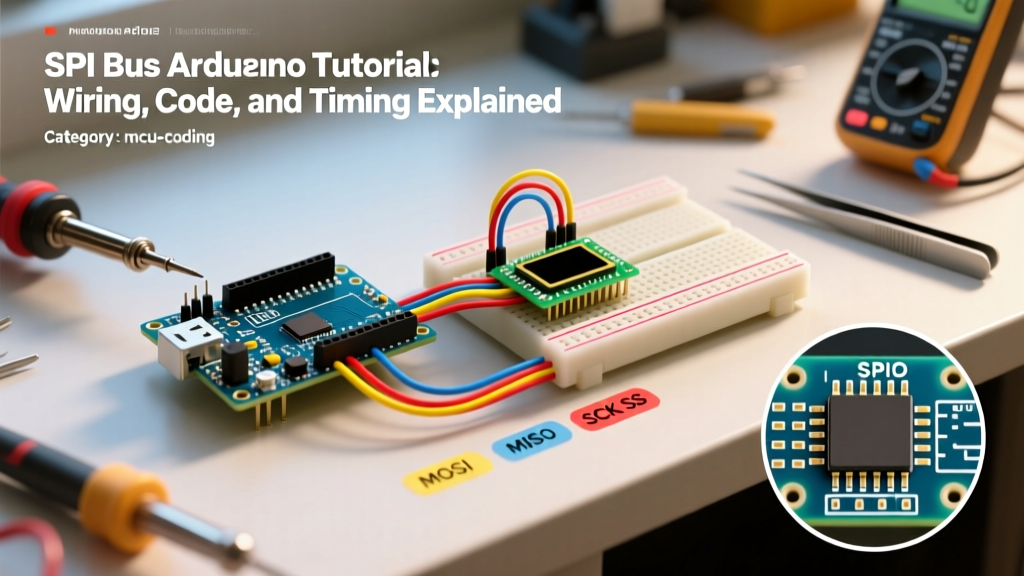
Standard SPI utilizes four primary logic lines to establish communication between a single Controller (the Arduino) and one or more Peripherals (sensors, displays, or memory chips).
- SCK (Serial Clock): Generated by the Controller. This line dictates the exact timing for when bits are shifted in and out.
- MOSI (Controller Out, Peripheral In): The data line used to send information from the Arduino to the peripheral.
- MISO (Controller In, Peripheral Out): The data line used to receive information from the peripheral back to the Arduino.
- CS/SS (Chip Select / Slave Select): An active-low signal used to wake up a specific peripheral. Because SPI lacks the addressing scheme of I2C, every peripheral requires its own dedicated CS pin.
Default SPI Pinouts for Modern Arduino Boards
While you can use software SPI (bit-banging) on any GPIO pins, hardware SPI is routed to specific pins tied to the microcontroller's internal SPI peripheral. Here is the standard mapping for the most common boards used by hobbyists and engineers today:
| Board Model | SCK | MISO | MOSI | Default CS | Logic Level |
|---|---|---|---|---|---|
| Arduino Uno R4 Minima | D13 | D12 | D11 | D10 | 5.0V |
| Arduino Nano ESP32 | D13 | D12 | D11 | D10 | 3.3V |
| Arduino Mega 2560 | D52 | D50 | D51 | D53 | 5.0V |
Clock Polarity and Phase: The CPOL/CPHA Matrix
One of the most frequent stumbling blocks for beginners is configuring the clock mode. Because SPI is not governed by a single universal standard like I2C, different silicon manufacturers implement different timing requirements. This is defined by two parameters: Clock Polarity (CPOL) and Clock Phase (CPHA).
Expert Insight: Always consult the timing diagram in your peripheral's datasheet. Guessing the SPI mode will result in corrupted data or complete communication failure. According to Analog Devices, mismatched clock phases are the leading cause of integration errors in mixed-signal PCB designs.
| SPI Mode | CPOL (Clock Idle State) | CPHA (Data Sampling Edge) | Common Use Cases |
|---|---|---|---|
| Mode 0 | LOW (0) | Rising Edge | Winbond Flash, Most SD Cards, MAX7219 |
| Mode 1 | LOW (0) | Falling Edge | Certain ADCs, Legacy Sensors |
| Mode 2 | HIGH (1) | Falling Edge | Some STMicroelectronics accelerometers |
| Mode 3 | HIGH (1) | Rising Edge | Many Bosch sensors (BME280), Shift Registers |
Step-by-Step: Interfacing a W25Q32 SPI Flash Chip
To demonstrate a real-world implementation, we will interface an Arduino Uno R4 with a W25Q32 SPI Flash Memory chip. This is a ubiquitous, low-cost ($0.40 to $0.80 in bulk) 32-megabit storage IC used for data logging.
The Logic Level Danger Zone
The W25Q32 operates strictly at 3.3V logic and power. If you are using a 5V Arduino board (like the Uno R4 or Mega), sending 5V signals directly into the MISO, MOSI, SCK, and CS pins will degrade the silicon over time and may instantly destroy the chip's input buffers. You must use a bidirectional logic level shifter, such as the 74AHCT125 or a dedicated BSS138 MOSFET-based level shifter module ($2.50 average retail price), to safely translate the 5V signals down to 3.3V.
Writing Bulletproof SPI Code in 2026
In older tutorials, you might see functions like SPI.setClockDivider(). This is deprecated and dangerous in modern environments because it does not protect against interrupt conflicts. If an interrupt fires while an SPI transaction is occurring, it could change the clock speed and corrupt the data stream.
The modern, robust approach utilizes the SPI.beginTransaction() and SPI.endTransaction() API. This ensures that your specific peripheral settings are locked in and protected from other libraries (like an Ethernet shield or SD card module) that might try to hijack the Arduino SPI bus.
#include <SPI.h>

// Define the Chip Select pin
const int CS_PIN = 10;

void setup() {
  Serial.begin(115200);
  while (!Serial); // Wait for serial monitor

  // Initialize the CS pin as OUTPUT and set HIGH (deselect)
  pinMode(CS_PIN, OUTPUT);
  digitalWrite(CS_PIN, HIGH);

  // Initialize the hardware SPI bus
  SPI.begin();
  Serial.println("SPI Bus Initialized.");
}

void loop() {
  // Define transaction settings: 16MHz, MSB First, Mode 0
  SPISettings mySettings(16000000, MSBFIRST, SPI_MODE0);

  // Begin transaction to lock in settings and block interrupts
  SPI.beginTransaction(mySettings);
  digitalWrite(CS_PIN, LOW); // Wake up the W25Q32

  // Send the JEDEC ID command (0x9F)
  SPI.transfer(0x9F);

  // Read back 3 bytes: Manufacturer ID, Memory Type, Capacity
  byte manufacturer = SPI.transfer(0x00);
  byte memType = SPI.transfer(0x00);
  byte capacity = SPI.transfer(0x00);

  digitalWrite(CS_PIN, HIGH); // Deselect the chip
  SPI.endTransaction(); // Release the bus

  Serial.print("Manufacturer ID: 0x");
  Serial.println(manufacturer, HEX);
  Serial.print("Memory Type: 0x");
  Serial.println(memType, HEX);
  Serial.print("Capacity: 0x");
  Serial.println(capacity, HEX);

  delay(3000); // Read every 3 seconds
}
Code Breakdown and Timing Specifics
- SPISettings Object: We define a 16 MHz clock. The W25Q32 supports up to 104 MHz for fast-read instructions, but 16 MHz is the safe maximum for standard breadboard wiring due to parasitic capacitance.
- Chip Select Management: Notice that
digitalWrite(CS_PIN, LOW)happens afterbeginTransaction(). This is crucial. Some peripherals will begin shifting data out on the MISO line the exact nanosecond CS goes low, even before the first clock pulse. - Dummy Bytes: When we call
SPI.transfer(0x00)to read data, we are actually sending zeros to the flash chip. Because SPI is full-duplex, the Controller must send a byte to generate the 8 clock pulses required to receive a byte back.
Protocol Comparison Matrix
Why choose SPI over other protocols? Here is a rapid comparison to help you make architectural decisions for your next project.
| Feature | SPI | I2C | UART |
|---|---|---|---|
| Wiring Complexity | 4 wires + 1 per peripheral (CS) | 2 wires (Shared) | 2 wires (Point-to-Point) |
| Max Speed (Typical) | 10 MHz - 50 MHz | 100 kHz - 3.4 MHz | 115.2 kbps - 2 Mbps |
| Duplex | Full-Duplex | Half-Duplex | Full-Duplex |
| Addressing | Hardware CS lines | 7-bit / 10-bit Software | None (Point-to-Point) |
Troubleshooting Common SPI Failures
When your SPI bus Arduino setup fails to communicate, the issue is rarely in the code. It is almost always a physical layer violation. Use this checklist to debug your hardware:
1. Parasitic Capacitance and Wire Length
SPI is designed for on-PCB communication or very short jumper wires. At 16 MHz, the square wave clock signal contains high-frequency harmonics. If your jumper wires exceed 15 cm (6 inches), the capacitance between the wires will round off the sharp edges of the clock signal. The peripheral will fail to register the clock edge, resulting in bit-shifts. Fix: Keep SPI traces under 10 cm, or lower the clock speed to 4 MHz for longer runs.
2. Ground Bounce on the CS Line
If you are switching high-current loads (like motors or LED strips) on the same breadboard, the ground plane may experience voltage spikes. If the ground reference bounces above 0.8V, the peripheral might interpret the CS line as going HIGH (deselecting) in the middle of a transaction. Fix: Use a dedicated ground wire directly from the Arduino GND pin to the peripheral GND pin, avoiding shared breadboard power rails.
3. MISO Tri-State Conflicts
If you have multiple SPI devices on the same bus, their MISO lines are tied together. When a device's CS pin is HIGH, its MISO pin must enter a high-impedance (tri-state) mode. If you are using a cheap, generic breakout board that lacks proper tri-state buffer logic on the MISO line, it will block all other devices on the bus. Fix: Test each peripheral individually, or add a 74HC125 tri-state buffer to the MISO line of the offending module.
Final Thoughts on SPI Architecture
Mastering the SPI bus requires a shift in mindset from software-only logic to hardware-aware programming. By respecting logic voltage thresholds, understanding clock phase timing, and utilizing the modern transaction-based API, you will build embedded systems that are resilient, fast, and immune to the intermittent data corruption that plagues beginner projects. Always keep the datasheet open on your second monitor, and trust the oscilloscope over your assumptions.