
Beyond Wire.begin(): The Reality of Arduino I2C Hardware
When makers first learn about the Inter-Integrated Circuit (I2C) protocol, they are often taught that it is a simple two-wire bus requiring only SDA (data) and SCL (clock) lines. While the Arduino Wire Library Reference abstracts away the complexity with a simple Wire.begin() call, treating I2C as a plug-and-play software abstraction leads to catastrophic failures in complex projects. As we move through 2026, the Arduino ecosystem has expanded far beyond the legacy ATmega328P (Uno R3). Modern boards like the Arduino Uno R4 Minima (powered by the Renesas RA4M1 ARM Cortex-M4) and RP2040-based boards utilize entirely different hardware I2C peripherals, meaning the underlying behavior of the Wire.h library varies significantly depending on your silicon.
This deep dive bypasses the beginner tutorials and dissects the actual hardware limitations, bus physics, and advanced debugging techniques required to build robust, multi-sensor I2C networks that won't lock up in the field.
Deconstructing the Wire.h API and Buffer Limits
The most common point of failure in Arduino I2C communication is the transmit buffer overflow. The Wire object does not send data over the bus the moment you call Wire.write(). Instead, it queues bytes into a static memory buffer. When you call Wire.endTransmission(), the hardware TWI (Two-Wire Interface) or I2C peripheral flushes this buffer to the slave device.
If you are migrating code from an older Uno R3 to a modern 32-bit board, you must account for differing buffer sizes:
- AVR (ATmega328P / Uno R3): 32-byte TX and RX buffers.
- ARM / RP2040 / Renesas (Uno R4, Nano 33 IoT, Pico): Typically 256-byte TX and RX buffers.
Attempting to send a 64-byte payload to an OLED display in a single transaction on an AVR board will silently truncate your data, resulting in corrupted graphics. Always break large payloads into 16-byte or 32-byte chunks.
Decoding Wire.endTransmission() Return Codes
Most hobbyist code ignores the return value of Wire.endTransmission(). In industrial or reliable deployments, you must evaluate this byte to handle bus errors gracefully.
| Return Code | Meaning | Actionable Fix |
|---|---|---|
| 0 | Success | None required. |
| 1 | Data too long to fit in transmit buffer | Chunk your Wire.write() calls into smaller batches. |
| 2 | Received NACK on transmit of address | Verify slave address, check pull-up resistors, ensure slave is powered. |
| 3 | Received NACK on transmit of data | Slave rejected the payload; check slave register map and state. |
| 4 | Other error (e.g., bus arbitration lost) | Check for multi-master conflicts or severe noise on SDA/SCL lines. |
The Physics of the Bus: Pull-Up Resistors and Capacitance
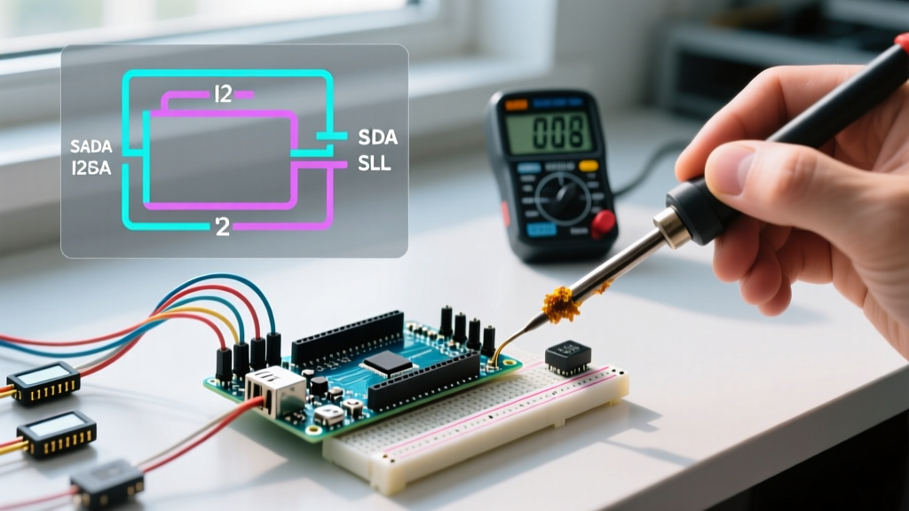
I2C is an open-drain (or open-collector) bus. The master and slaves can only pull the SDA and SCL lines LOW (to ground); they cannot drive them HIGH. To achieve a HIGH state, external pull-up resistors are required to pull the voltage back to VCC. As detailed in the SparkFun I2C Tutorial, choosing the wrong resistor value is the root cause of 90% of I2C communication errors at higher speeds.
Calculating the Minimum Pull-Up Resistance
If your pull-up resistor is too small (low resistance), the current sink inside the microcontroller will be overwhelmed when it tries to pull the line LOW, potentially damaging the silicon or failing to reach the logical LOW threshold ($V_{OL}$). The formula for the minimum resistor value is:
Rp(min) = (VCC - VOL) / IOL
Where VOL is typically 0.4V and IOL is the maximum sink current (usually 3mA for standard I2C).
For a 5V system (Uno R3): Rp(min) = (5 - 0.4) / 0.003 = 1,533 Ω.
For a 3.3V system (Uno R4 / RP2040): Rp(min) = (3.3 - 0.4) / 0.003 = 966 Ω.
This means using a standard 1kΩ pull-up on a 5V system is dangerous, but perfectly safe on a 3.3V system.
Bus Capacitance and Rise Time
Every wire, breadboard contact, and sensor pin adds parasitic capacitance to the bus. The I2C specification limits standard bus capacitance to 400 pF. When combined with the pull-up resistor, this creates an RC low-pass filter. If the resistance is too high (e.g., 10kΩ), the voltage rise time will be too slow, and the microcontroller will misinterpret the signal at 400 kHz (Fast Mode). For 400 kHz operation on a bus with multiple sensors, drop your pull-ups from the default 4.7kΩ to 2.2kΩ to ensure sharp signal edges.
Clock Stretching: The Silent Bus Killer
Clock stretching occurs when a slave device needs more time to process data. It holds the SCL line LOW, forcing the master to wait before sending the next clock pulse. While this is a valid part of the I2C protocol, it is notoriously problematic on older AVR-based Arduinos.
The hardware TWI peripheral on the ATmega328P has a known silicon errata regarding clock stretching; if the slave holds SCL low for too long, the TWI state machine can lock up indefinitely, requiring a hard microcontroller reset. Modern 32-bit boards like the Arduino Uno R4 and Nano ESP32 handle clock stretching natively in hardware without hanging. If you are forced to use an AVR board with a slow sensor (like certain high-resolution ADCs or SMBus-compatible battery management chips), you must implement software timeouts using Wire.setWireTimeout(25000, true) (available in newer AVR cores) to prevent permanent bus lockups.
Advanced Debugging: When the Bus Locks Up
In a real-world deployment, electrical noise or a sudden power brownout can cause the master and slave to lose synchronization. A classic failure mode is the SDA Stuck Low condition. This happens if the master reboots or loses power while a slave is in the middle of transmitting a byte (specifically, while the slave is outputting a '0' bit). The slave will continue holding SDA low, waiting for clock pulses that the rebooted master is no longer sending. When the master boots and initializes the I2C peripheral, it will detect the bus as 'busy' and refuse to communicate.
The 9-Clock Pulse Recovery Trick
To recover from an SDA Stuck Low condition without power-cycling the entire system, you must manually clock the slave out of its transmission state. Since the hardware I2C peripheral refuses to toggle SCL when it thinks the bus is busy, you must temporarily hijack the SCL pin as a standard GPIO output.
- Detach the I2C peripheral from the SCL pin.
- Configure the SCL pin as a standard digital
OUTPUT. - Toggle the SCL pin HIGH and LOW exactly 9 times. (8 bits for the data byte, plus 1 for the ACK/NACK bit).
- Send a manual STOP condition (SDA goes from LOW to HIGH while SCL is HIGH).
- Re-initialize the I2C peripheral using
Wire.begin().
This forces the slave to finish its pending byte and release the SDA line, restoring bus functionality.
Hardware Tools for I2C Analysis
When software debugging fails, you must look at the physical layer. According to the Analog Devices I2C Primer, oscilloscopes and logic analyzers are mandatory for diagnosing rise-time and noise issues.
- Entry-Level ($12 - $20): FX2LA-based logic analyzer clones. While lacking advanced triggers, they are sufficient for capturing 100 kHz I2C traffic and decoding addresses using PulseView or Sigrok.
- Professional ($119+): Saleae Logic Pro 8. Offers pristine 50 MS/s sampling, hardware I2C decoding, and the ability to trigger on specific NACKs or missing ACKs, which is invaluable for catching intermittent bus errors.
- Oscilloscope ($299+): A rig like the Siglent SDS1202X-E is necessary to measure the actual analog rise time (in nanoseconds) of the SDA line to verify if your pull-up resistors are correctly sized for the bus capacitance.
Frequently Asked Questions
Can I mix 5V and 3.3V I2C devices on the same Arduino bus?
Not directly. While the I2C protocol is open-drain, a 5V master pulling the line HIGH will feed 5V into the SDA pin of a 3.3V slave, potentially destroying it. You must use a dedicated bidirectional logic level shifter (like the BSS138 MOSFET-based shifters, costing roughly $2) to isolate the 5V and 3.3V pull-up domains safely.
Why does my I2C bus work on a breadboard but fail when soldered to a PCB?
Breadboards add significant parasitic capacitance and contact resistance, which can sometimes accidentally dampen high-frequency ringing. Conversely, long, unshielded wires on a PCB can act as antennas for EMI. If a PCB fails while a breadboard works, check your ground plane integrity, ensure pull-up resistors are placed physically close to the master, and verify that SDA and SCL traces are not routed parallel to high-current switching nodes (like buck converter inductors).
How do I change the I2C address of a sensor if it conflicts with another?
I2C addresses are hardcoded in silicon, but many sensors (like the BME280 or MPU6050) feature an SDO/SA0 pin. Tying this pin to VCC or GND shifts the address by one bit (e.g., 0x76 vs 0x77). If your sensor lacks this pin and conflicts with another device, you must use an I2C multiplexer like the TCA9548A (approx. $3.50) to create isolated sub-buses, allowing you to run multiple identical sensors on the same master.