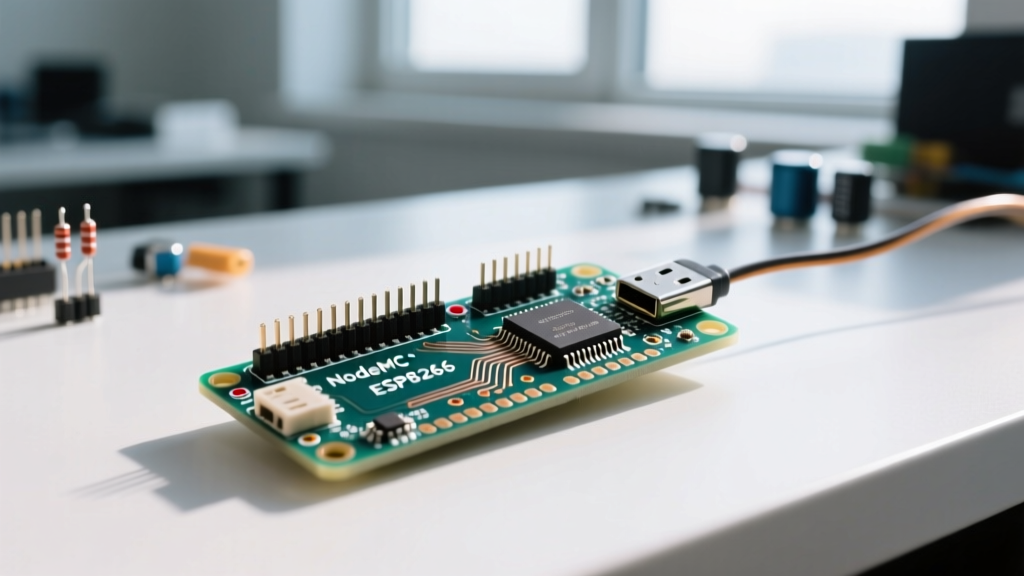

The NodeMCU pin layout is the physical mapping scheme that translates the ESP8266 microcontroller's internal GPIO numbers into the user-friendly silk-screened labels (like D1, D2) on the development board. Understanding this layout changes how you declare pins in your Arduino IDE code and dictates which physical pins you can safely wire to relays or sensors without bricking the boot sequence. Beginners most commonly confuse the physical silk-screen label (e.g., D3) with the internal ESP8266 GPIO number (e.g., GPIO0), or mistakenly assume an ESP32 NodeMCU board shares this exact same D-pin layout.
The Core NodeMCU Pin Layout Mapping Table
Before wiring any peripheral, you must cross-reference the silk-screened D-pins with the ESP8266's internal GPIO numbers. The table below maps the physical board labels to their internal architecture, default boot states, and special hardware functions. Keep this reference on your bench when designing sensor shields or relay boards.
| Silkscreen Label | Internal GPIO | Boot State Requirement | Special Function / Notes |
|---|---|---|---|
| D0 | GPIO16 | No restriction | Wake from deep sleep (must tie to RST); no PWM or I2C support. |
| D1 | GPIO5 | No restriction | Default I2C SCL pin; safe for general I/O and PWM. |
| D2 | GPIO4 | No restriction | Default I2C SDA pin; safe for general I/O and PWM. |
| D3 | GPIO0 | MUST BE HIGH | Boot mode select. If LOW at boot, enters UART flash mode. Has internal pull-up. |
| D4 | GPIO2 | MUST BE HIGH | TX1 (secondary serial). Has internal pull-up. Built-in LED on some v2 boards. |
| D5 | GPIO14 | No restriction | Default SPI SCK pin; excellent for general I/O and PWM. |
| D6 | GPIO12 | No restriction | Default SPI MISO pin; safe for general I/O. |
| D7 | GPIO13 | No restriction | Default SPI MOSI pin; safe for general I/O and PWM. |
| D8 | GPIO15 | MUST BE LOW | Default SPI SS (CS) pin. If HIGH at boot, halts execution. Has internal pull-down. |
| A0 | ADC (TOUT) | N/A | Analog input. Board has internal voltage divider; max safe input is 3.3V. |
D1 macros directly if the NodeMCU board package is installed (e.g., pinMode(D1, OUTPUT);). However, if you are writing a library intended to be cross-compatible with raw ESP-12F modules, always use the raw GPIO numbers (e.g., pinMode(5, OUTPUT);).
What This Changes in Your Circuit and Code
The most critical hardware translation in the NodeMCU pin layout involves the analog input pin (A0). The raw ESP8266 silicon features a single 10-bit ADC channel (TOUT) that maxes out at 1.0V. If you feed 3.3V directly into a raw ESP-12F module's TOUT pin, you will saturate the reading and risk damaging the silicon.
To solve this, NodeMCU development boards (like the widely used LoLin v3 and Amica variants) integrate an internal voltage divider on the A0 trace. This divider typically consists of a 220kΩ and a 100kΩ resistor. This changes how you must calculate sensor inputs in your circuit design.
Numeric Example: Calculating the A0 Voltage Divider
Let's calculate the actual voltage reaching the ESP8266 silicon when you apply the maximum safe board-level voltage of 3.3V to the A0 pin.
- Formula:
V_out = V_in × (R2 / (R1 + R2)) - Values:
V_in = 3.3V,R1 = 220,000Ω,R2 = 100,000Ω - Calculation:
3.3 × (100,000 / 320,000) = 3.3 × 0.3125 = 1.031V
The internal pin sees ~1.03V, which is safely within the 1.0V-1.1V tolerance of the ESP8266 ADC. In your Arduino code, the analogRead(A0) function automatically maps this 0-1.03V range to a 10-bit integer (0-1023).
Never feed a 5V signal (like from an Arduino Uno or a 5V soil moisture sensor) into the NodeMCU A0 pin.
Math:
5.0V × 0.3125 = 1.56V. This pushes 1.56V into a 1.0V-rated internal pin, which will permanently skew your ADC calibration or destroy the internal multiplexer. Always use an external resistor divider to step 5V signals down to 3.3V before they hit the NodeMCU board.
Where You Meet This in Practice: Boot Strapping Hazards
The most common point of failure for hobbyists wiring relays, motor drivers, or switches to a NodeMCU is ignoring the boot-strapping requirements of pins D3 (GPIO0), D4 (GPIO2), and D8 (GPIO15).
During the first 100 milliseconds of power-on, the ESP8266 reads the voltage state of these specific pins to decide how to boot. According to the Espressif Hardware Design Guidelines, the chip samples these pins to determine the boot mode:
- D3 (GPIO0): Must be HIGH to boot normally. If pulled LOW (e.g., by a pressed button or a relay module with a default LOW state), the chip enters UART Serial Bootloader mode to receive new firmware. Your code will not run.
- D4 (GPIO2): Must be HIGH to boot normally. This pin has an internal pull-up resistor, so it is generally safe unless you wire an external pull-down resistor or a load that sinks current heavily on startup.
- D8 (GPIO15): Must be LOW to boot normally. This pin has an internal pull-down resistor. If you wire a relay module with an optocoupler that pulls this pin HIGH during the 3.3V ramp-up phase, the ESP8266 will halt execution entirely and output garbage to the serial monitor.
Practical Rule of Thumb: Reserve D3, D4, and D8 strictly for I2C sensors, SPI peripherals (where CS is managed by the master), or input buttons that are guaranteed to be open-circuit during power-on. Use D1, D2, D5, D6, and D7 for relays, solenoids, and motor drivers.
Power Delivery and Pin Current Limits
Understanding the NodeMCU pin layout also means understanding its power architecture. The board is typically powered via the micro-USB port (5V) or the VIN pin. The onboard LDO regulator (usually an AMS1117-3.3) steps this down to 3.3V.
- 3V3 Pin Max Output: ~800mA (absolute limit of AMS1117), but practical continuous draw should stay under 500mA to prevent thermal shutdown.
- Single GPIO Pin Source/Sink: 12mA recommended continuous (absolute max 20mA per NodeMCU GPIO documentation).
- Total GPIO Current: All GPIO pins combined should not exceed 50mA aggregate.
- VIN Pin: Passes raw USB voltage (typically 4.8V - 5.2V). Do not use this to power 3.3V logic directly.
If your circuit requires driving a 5V relay coil (which typically draws 70mA to 90mA), you cannot power it from the NodeMCU's 3V3 pin, nor can you trigger it directly from a GPIO pin. You must use the VIN pin to power the relay's VCC, and use an N-channel MOSFET (like a 2N7000) or an optocoupler triggered by a safe GPIO pin (like D5) to switch the relay ground.
Frequently Asked Questions
Can I use D0 (GPIO16) to drive a relay or read a button?
You can use D0 to read a button or drive a relay, but D0 does not support hardware PWM or interrupt-driven attachInterrupt() functions in the standard ESP8266 Arduino core. Furthermore, D0 is the only pin that can wake the ESP8266 from deep sleep; to use this feature, you must physically wire D0 to the RST pin on the board.
Why does my I2C sensor fail when wired to D1 and D2?
D1 (SCL) and D2 (SDA) are the default I2C pins. If your I2C sensor module already has onboard 4.7kΩ pull-up resistors tied to 5V, connecting it to the NodeMCU will backfeed 5V into the ESP8266's 3.3V GPIO pins via the I2C lines. This can cause erratic behavior or silicon damage. Always verify your sensor module's pull-up voltage, or remove the surface-mount pull-up resistors from the sensor module and rely on the ESP8266's internal weak pull-ups (or add external 4.7kΩ resistors tied to the NodeMCU's 3V3 pin).
Is the NodeMCU ESP32 pin layout the same?
No. "NodeMCU" refers to a specific open-source firmware and the physical breadboard-friendly form factor. While manufacturers produce "NodeMCU-style" boards using the ESP32 chip, the ESP32 has a completely different internal architecture. ESP32 boards do not use the D0-D8 silkscreen naming convention; they label pins directly by their GPIO numbers (e.g., GPIO21, GPIO22 for I2C). Always check the specific silicon datasheet for the board you are holding.