
The Dual Datasheet Reality: Board vs. Silicon
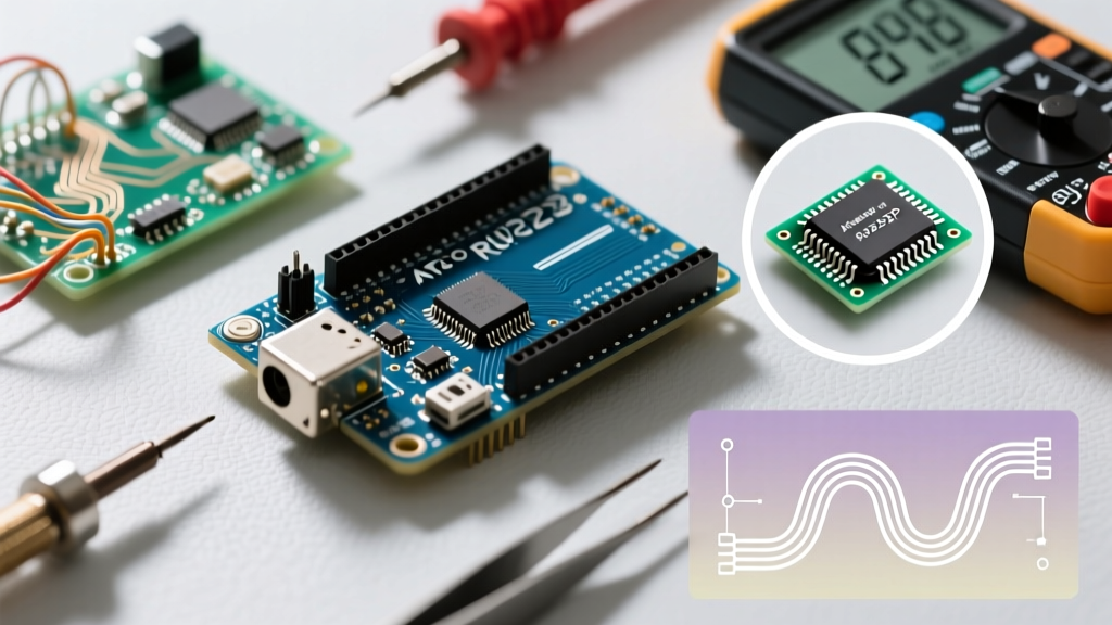
When engineers and makers search for the Arduino Uno R3 datasheet, they are often conflating two entirely different documents. To truly master this platform and integrate it into a broader hardware ecosystem, you must distinguish between the board-level schematic and the silicon-level datasheet. The board-level documentation outlines the physical layout, voltage regulators, and the R3-specific pinout additions (like the IOREF and dedicated SDA/SCL headers). The silicon-level documentation belongs to the Microchip ATmega328P microcontroller, detailing register maps, clock tolerances, and absolute maximum electrical ratings.
Even in 2026, with the prevalence of the Uno R4 and ESP32-based alternatives, the Uno R3 form factor remains the undisputed mechanical and electrical standard for educational kits, legacy industrial shields, and rapid prototyping. Understanding the hard limits defined in these combined datasheets is the difference between a reliable deployment and a catastrophic thermal failure.
Expert Note: The 'R3' designation specifically refers to the third major revision of the board. It introduced the ATmega16U2 USB-to-Serial chip (replacing the 8U2), added the IOREF pin for shield voltage adaptation, and brought I2C (SDA/SCL) pins to the main digital header. If your project relies on I2C shields, verifying R3 compliance is mandatory.
Power Architecture and Thermal Dissipation Limits
The most misunderstood section of the Arduino Uno R3 hardware documentation is the power regulation circuit. The board utilizes an NCP1117ST50T3G low-dropout (LDO) linear regulator to step down the external barrel jack voltage to 5V. While the marketing materials suggest an input range of 7V to 12V, the physical datasheet and thermal physics tell a more restrictive story.
The NCP1117 is housed in a SOT-223 package. Without a dedicated heatsink, its thermal resistance to ambient air is roughly 100°C/W. When you supply 12V to the barrel jack and draw current from the 5V pin, the LDO must dissipate the voltage difference as heat.
Thermal Failure Matrix: Barrel Jack Input vs. 5V Draw
| Input Voltage (Vin) | Voltage Drop | Current Draw (5V Pin) | Power Dissipated | Estimated Temp Rise | Ecosystem Risk Level |
|---|---|---|---|---|---|
| 7.0V | 2.0V | 100 mA | 0.20W | +20°C | Safe (Warm to touch) |
| 9.0V | 4.0V | 100 mA | 0.40W | +40°C | Moderate (Hot, safe for short durations) |
| 12.0V | 7.0V | 100 mA | 0.70W | +70°C | Critical (Thermal shutdown likely, burn risk) |
| 12.0V | 7.0V | 300 mA | 2.10W | +210°C | Catastrophic (Immediate LDO failure) |
Actionable Advice: If your shield ecosystem requires more than 150mA of 5V power (e.g., driving multiple servos or high-brightness LED matrices), bypass the onboard LDO entirely. Use a dedicated buck converter module to supply 5V directly to the board's 5V pin, ensuring the USB cable is disconnected to prevent back-feeding the PC's USB bus.
I/O Pinout Ecosystem: The 200mA Package Limit
A common trap for intermediate developers is reading the ATmega328P datasheet and seeing that each I/O pin can source or sink up to 40mA (absolute maximum). However, the official Arduino hardware documentation and the silicon datasheet both specify a strict 200mA total package limit for the VCC and GND pins combined.
Calculating Real-World I/O Headroom
- The Microcontroller Baseline: The ATmega328P itself consumes roughly 15mA to 20mA at 16MHz and 5V just to execute code.
- The USB-to-Serial Tax: The ATmega16U2 chip and the TX/RX LEDs draw an additional 10mA to 15mA.
- Available Headroom: This leaves approximately 165mA for your external peripherals before you risk melting the internal bond wires of the DIP package.
If you connect 10 LEDs and drive them at 20mA each, you are pulling 200mA. Add the board's baseline consumption, and you exceed the 200mA absolute maximum. The immediate failure mode is not always a dead chip; often, it manifests as erratic brownout resets, corrupted EEPROM data, or a degraded voltage regulator output.
Clock Tolerance: Ceramic Resonator vs. Quartz Crystal
An often-overlooked detail in the Uno R3 schematic is the clock source. Unlike early Arduino boards that used a 16MHz quartz crystal, the genuine Uno R3 utilizes a 16MHz ceramic resonator (typically a Murata CSTCE series).
Quartz crystals offer a frequency tolerance of around ±30 ppm (parts per million). Ceramic resonators have a much looser tolerance of ±0.5% (5000 ppm). For standard GPIO toggling or reading sensors over I2C, this is irrelevant. However, if your ecosystem relies on high-speed asynchronous UART communication (e.g., pushing 1Mbps or 2Mbps baud rates to a secondary microcontroller or a PC), the ceramic resonator's drift can cause framing errors and dropped packets. When designing custom shields that require high-speed serial sync, always implement hardware flow control or use the SPI/I2C buses instead of relying on the R3's UART.
Where the Uno R3 Fits in the 2026 Hardware Landscape
How does the legacy R3 compare to modern alternatives when designing a new product ecosystem? Below is a technical comparison of the R3 against current market staples.
| Feature | Arduino Uno R3 (Genuine) | Arduino Uno R4 Minima | ESP32-C3 SuperMini |
|---|---|---|---|
| Core Silicon | ATmega328P (8-bit AVR) | Renesas RA4M1 (32-bit ARM Cortex-M4) | ESP32-C3 (32-bit RISC-V) |
| Clock Speed | 16 MHz | 48 MHz | 160 MHz |
| Logic Levels | 5V Tolerant | 5V Tolerant | 3.3V (Not 5V Tolerant) |
| Typical 2026 Price | $27.00 - $32.00 | $19.00 - $22.00 | $3.50 - $5.00 |
| Shield Ecosystem | Native 100% Compatible | Native 100% Compatible | Requires Level Shifters |
| DAC / Op-Amp | None | 12-bit DAC, Internal Op-Amp | None |
While the ESP32-C3 dominates in raw compute and IoT connectivity for under $5, it lacks 5V logic tolerance. Interfacing an ESP32 with the vast ecosystem of legacy 5V Arduino shields requires bulky bidirectional logic level shifters, which introduce signal propagation delays. The Uno R3, despite its aged 8-bit architecture, remains the most frictionless platform for interfacing with 5V industrial sensors, automotive relays, and legacy displays without additional support circuitry.
Critical Failure Modes to Avoid
Based on field returns and community post-mortems, here are the most common ways developers destroy the Uno R3 by ignoring its hardware documentation:
- Backfeeding the 5V Pin: Supplying 5V to the '5V' pin while simultaneously plugging in the USB cable. The board lacks a physical switch or ideal diode to isolate the USB VBUS from the 5V header. This creates a voltage contention loop that will fry the USB port on your PC or the ATmega16U2 chip.
- Exceeding the 3.3V Regulator Limit: The onboard 3.3V output is derived from the USB-to-Serial chip's internal regulator (on genuine boards) or a secondary LDO (on clones). It is typically rated for a maximum of 50mA to 150mA. Plugging in a modern, power-hungry 3.3V sensor array will brown out the USB interface, causing the PC to repeatedly disconnect and reconnect the COM port.
- Inductive Kickback on Digital Pins: Driving relays or solenoids directly from the digital I/O pins without a flyback diode. The ATmega328P's internal ESD protection diodes will absorb the initial inductive spike, but repeated hits will latch up the silicon, permanently shorting the I/O port to VCC.
Final Verdict for System Integrators
The Arduino Uno R3 is no longer the cutting edge of embedded compute, but it is the bedrock of physical computing interoperability. By thoroughly reviewing both the board-level schematics and the ATmega328P silicon datasheet, engineers can safely push the platform to its absolute limits. Respect the thermal boundaries of the NCP1117 LDO, manage your total package current draw, and leverage the IOREF pin for seamless shield integration. When applied correctly, the R3 ecosystem remains an incredibly robust, predictable, and cost-effective foundation for both prototyping and low-volume production deployments.