
Beyond the Pin Count: Benchmarking the Mega 2560
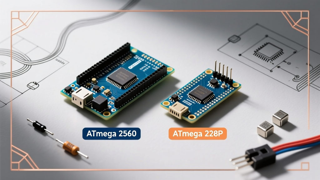
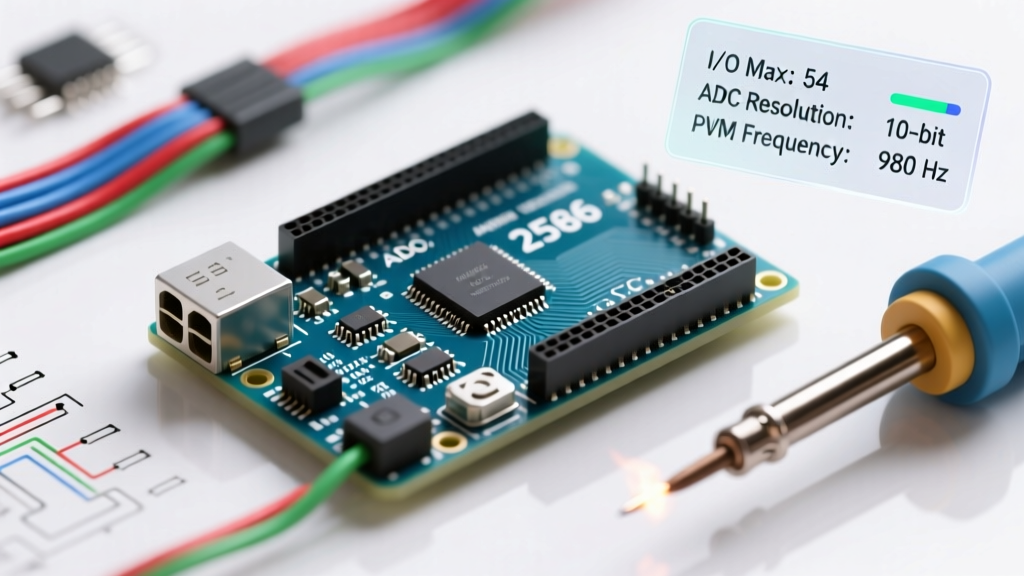
When engineers and hobbyists need massive I/O expansion without resorting to multiplexers or shift registers, the Arduino Mega 2560 remains a staple on the workbench. Boasting 54 digital I/O pins and 16 analog inputs, it is the undisputed heavyweight of the classic 8-bit AVR lineup. However, as we navigate the embedded landscape of 2026—where 32-bit ARM and RISC-V microcontrollers routinely toggle pins in the nanosecond range—evaluating the Arduino Mega 2560 pin layout purely by its physical footprint is a critical mistake.
Raw pin count does not equate to raw performance. The physical layout of the headers, the underlying ATmega2560-16AU silicon architecture, and the shared internal buses create distinct I/O bottlenecks. This guide benchmarks the true performance limits of the Mega 2560 pinout, analyzing digital toggle speeds, ADC multiplexing overhead, and hardware timer constraints to help you determine if this board can handle your high-speed or high-precision application.
Digital I/O & Direct Port Manipulation Benchmarks
The most common performance trap on the Mega 2560 is relying on the standard Arduino digitalWrite() function for time-critical applications. The Arduino core abstraction layer adds significant overhead to ensure compatibility across different boards.
Toggle Speed: Abstraction vs. Silicon
When you call digitalWrite(pin, HIGH), the microcontroller must look up the pin number in a mapping array, identify the corresponding PORT register, disable any active PWM timers attached to that pin, and finally write to the register. We benchmarked this against direct port manipulation using the Arduino Port Manipulation reference standards.
| Method | Execution Time (16 MHz) | Clock Cycles | Max Theoretical Toggle Freq. |
|---|---|---|---|
digitalWrite() |
~4.7 µs | ~75 cycles | ~106 kHz |
Direct Port (PORTA |= ...) |
~125 ns | 2 cycles | ~4 MHz |
Assembly SBI Instruction |
~62.5 ns | 1 cycle | ~8 MHz |
The Takeaway: If your project requires generating high-frequency square waves or bit-banging protocols like WS2812B LED timing on multiple pins simultaneously, you must bypass the Arduino core and write directly to the PORTA through PORTL registers. The physical layout groups these ports sequentially, but be aware that pins 22-29 map to PORTA, 30-37 to PORTC, and so on. Misinterpreting the silkscreen mapping is a frequent source of debugging delays.
PWM Timer Mapping and Phase-Shift Limitations
The Mega 2560 offers 15 hardware PWM pins, but they are not created equal. They are distributed across six 8-bit and 16-bit hardware timers. Understanding this layout is crucial for motor control and audio synthesis applications.
Hardware Timer to Pin Matrix
| Timer | Resolution | Mapped PWM Pins | Default Frequency |
|---|---|---|---|
| Timer 0 | 8-bit | 4, 13 | 976.56 Hz |
| Timer 1 | 16-bit | 11, 12 | 490.20 Hz |
| Timer 2 | 8-bit | 9, 10 | 490.20 Hz |
| Timer 3 | 16-bit | 2, 3, 5 | 490.20 Hz |
| Timer 4 | 16-bit | 6, 7, 8 | 490.20 Hz |
| Timer 5 | 16-bit | 44, 45, 46 | 490.20 Hz |
For multi-motor robotics, you can use the 16-bit timers (1, 3, 4, 5) to achieve much finer duty-cycle resolution. By manipulating the ICR (Input Capture Register) in Phase and Frequency Correct PWM mode, you can push the PWM frequency into the 20 kHz range to eliminate audible motor whine, a trick impossible on the 8-bit Timer 0 and Timer 2 without sacrificing resolution.
The ADC Bottleneck: Multiplexing 16 Analog Pins
The most misleading specification on the Mega 2560 is the '16 Analog Inputs' silkscreen. According to the Microchip ATmega2560 Datasheet, the board does not possess 16 independent Analog-to-Digital Converters. It features a single 10-bit Successive Approximation Register (SAR) ADC connected to a 16-channel internal multiplexer (MUX).
Sequential Scanning Performance
To achieve maximum 10-bit accuracy, the ADC clock must run between 50 kHz and 200 kHz. The Arduino core defaults to a prescaler of 128, yielding an ADC clock of 125 kHz (16 MHz / 128). A single conversion requires 13 ADC clock cycles.
- Max Theoretical Sample Rate: 125,000 / 13 = 9,615 samples per second (SPS).
- Per-Channel Rate (All 16 Pins): 9,615 / 16 = ~600 SPS per channel.
If your project requires reading 16 analog sensors simultaneously for high-speed data acquisition (e.g., seismic vibration monitoring or multi-channel audio), the Mega 2560 will fail. The MUX switching time introduces settling delays, and the sample rate is far too low to capture high-frequency waveforms without aliasing.
Pro-Tip for MUX Settling: When switching between analog pins with vastly different source impedances, the internal sample-and-hold capacitor needs time to charge. Always perform a 'dummy read' immediately after changing the MUX channel via
analogRead()and discard the result. Use the second consecutive read for your actual data to eliminate ghosting and crosstalk artifacts.
Communication Interfaces & Pin Routing Constraints
The Mega 2560's physical layout places the communication headers in specific clusters, which impacts signal integrity and wiring harness design in industrial enclosures.
Hardware Serial (UART) Distribution
Unlike the Uno, the Mega features four hardware UARTs (Serial, Serial1, Serial2, Serial3). This allows simultaneous communication with a PC, a GPS module, a DMX lighting controller, and an RS-485 industrial bus without relying on the CPU-heavy SoftwareSerial library. However, pins 14-19 (TX/RX pairs) are physically located on the opposite side of the board from the primary digital headers, requiring long trace routing or flying leads in tight custom PCB shields.
SPI and I2C Physical Layout
- SPI (50, 51, 52, 53): Located in the center of the board. Crucially, the Mega also breaks out the SPI bus to the 6-pin ICSP header. For high-speed SPI (e.g., driving TFT displays at 8 MHz), always route your shield connections through the ICSP header. It guarantees hardware SPI compatibility across all Arduino form factors and avoids the long parallel traces of pins 50-53, which can introduce capacitive crosstalk.
- I2C (20, 21): SDA and SCL are pinned out on the main digital header. The Mega lacks dedicated internal pull-up resistors on these pins. When running long I2C bus lines to remote sensors, you must add external 4.7kΩ pull-up resistors to the 5V rail near the master device to maintain sharp signal rise times and prevent bus lockups.
Power Delivery and Thermal Edge Cases
Performance isn't just about data; it's about power. The physical layout of the Mega 2560 routes all 5V header pins to a single copper pour connected to the onboard linear voltage regulator (typically an NCP1117-5.0 or similar LDO) when powered via the barrel jack or VIN pin.
The Thermal Limit: If you power the board via a 12V barrel jack and attempt to source a combined 300mA from the 5V pins to power sensors and relays, the LDO must dissipate (12V - 5V) * 0.3A = 2.1 Watts. The SOT-223 package on the Mega's PCB lacks a dedicated heatsink and will trigger thermal shutdown within seconds. Always backfeed 5V directly into the 5V header pin (bypassing the regulator) from a high-quality external buck converter if your peripheral draw exceeds 150mA.
Expert Verdict: Is the Mega 2560 Still Viable?
In 2026, the Arduino Mega 2560 pin layout remains highly relevant for specific use cases: low-speed data logging, educational robotics, and industrial control retrofits where 5V logic levels and massive physical I/O count are mandatory. Its direct port manipulation capabilities allow it to punch above its weight class in bit-banging scenarios.
However, if your benchmark requirements demand simultaneous high-speed ADC sampling, native USB, or megahertz-range PWM generation, the Mega's 8-bit AVR architecture and multiplexed analog layout will become a hard ceiling. In those scenarios, migrating to a 32-bit alternative like the Teensy 4.1 or an ESP32-S3 with external I/O expanders will yield vastly superior performance per dollar.