
The Hidden Threat: When Positive Electric Charge Attacks
In the world of electrical wiring and DIY electronics, we are conditioned to think about the flow of electrons. However, some of the most catastrophic and confusing component failures are not caused by moving electrons, but by a deficit of them. A net positive electric charge represents an absence of electrons, and when this charge accumulates or is misdirected, it creates severe troubleshooting scenarios. Whether you are dealing with electrostatic discharge (ESD) that fries a microcontroller or a reverse-polarity fault that melts a voltage regulator, understanding the behavior of positive charge is critical for accurate diagnostics.
Unlike electron flow, which moves through the atomic lattice of a copper conductor, a positive electric charge often manifests as a static buildup on insulators or as 'holes' in semiconductor physics. When a technician approaches a workbench carrying a massive static charge, or when a battery is wired backward, the resulting equalization or forced current paths can destroy sensitive gate oxides and P-N junctions in milliseconds. This guide provides a deep-dive diagnostic framework for identifying, measuring, and mitigating faults rooted in positive charge accumulation and polarity errors.
Diagnostic Phase 1: Identifying Static Positive Charge Accumulation (ESD)
The triboelectric effect is the primary culprit behind static positive electric charge buildup in a DIY environment. When you walk across a nylon carpet or slide off a synthetic chair, your body loses electrons to the surrounding materials. This leaves your physical body with a massive net positive electric charge, often reaching potentials of +10,000V to +15,000V relative to the grounded workbench.
When you reach out to touch a bare CMOS chip, such as an ATmega328P or a 555 timer, the universe demands equilibrium. The intense electric field generated by your positively charged finger pulls electrons violently through the chip's internal structures. While the positive charge itself doesn't 'flow' into the chip, the electrostatic attraction causes a localized, high-current electron avalanche that punctures the microscopic silicon dioxide gate oxides.
Real-World Failure Mode: The Gate Oxide Puncture
MOSFETs and modern microcontrollers rely on gate oxides that are only a few nanometers thick. A static positive electric charge event can induce a voltage spike well beyond the 20V breakdown threshold of these layers. Once punctured, the gate shorts to the source or drain.
- Symptom: The microcontroller draws excessive quiescent current (e.g., pulling 500mA instead of 5mA) and becomes hot to the touch.
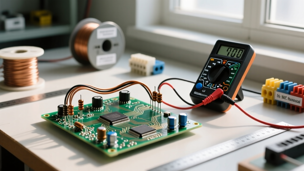
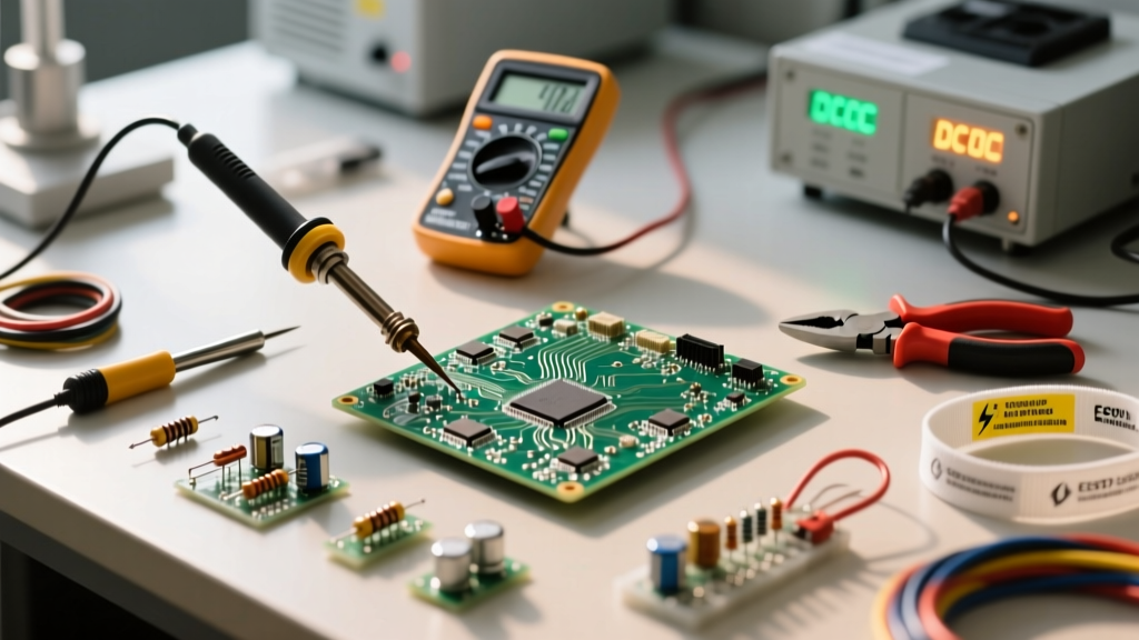
- Diagnostic Step: Set your Fluke multimeter to continuity or diode-test mode. Measure between the VCC and GND pins of the suspected IC. A dead short or a significantly lower forward voltage drop than the datasheet specifies indicates a ruptured gate oxide caused by ESD.
Diagnostic Phase 2: DC Polarity and 'Missing' Positive Charge Paths
In DC circuit troubleshooting, conventional current dictates that flow originates from the positive terminal. While physicists know electrons actually flow negative-to-positive, electrical schematics and diode symbols are entirely based on the movement of a theoretical positive electric charge. Confusing these paradigms leads to reverse polarity faults.
When a DIYer accidentally swaps the positive and negative leads on a barrel jack or a battery terminal, the circuit attempts to push a positive electric charge into the ground plane and pull it from the voltage rail. This forward-biases protection diodes that are meant to be reverse-biased, causing thermal runaway.
Troubleshooting Table: Polarity Fault vs. ESD Damage
| Diagnostic Metric | ESD (Static Positive Charge Event) | Reverse Polarity Fault |
|---|---|---|
| Visual Damage | None (internal microscopic damage) | Burnt traces, exploded electrolytic capacitors, charred ICs |
| Multimeter Reading (VCC to GND) | Dead short or abnormal diode drop | Shorted protection diode or melted trace continuity |
| Thermal Signature | Localized hot spot on specific IC | Widespread heat along power rails and bulk capacitors |
| Primary Culprit | Human Body Model (HBM) charge equalization | Incorrect wiring of DC source terminals |
Semiconductor Deep Dive: Holes as Positive Charge Carriers
To truly master electronics troubleshooting, you must understand how a positive electric charge moves inside a semiconductor. In P-type silicon, the charge carriers are not protons; they are 'holes'—the absence of an electron in the crystal lattice. These holes behave exactly like a positive electric charge, moving toward the negative terminal when a voltage is applied.
According to foundational texts on P-N junction semiconductor physics, the depletion region forms when electrons from the N-type material cross over to fill holes in the P-type material. If you are troubleshooting a failed rectifier diode or a BJT transistor, applying a reverse bias voltage widens this depletion region. If the reverse voltage exceeds the breakdown threshold (e.g., 50V for a 1N4001), the intense electric field rips electrons from their bonds, creating a massive avalanche of new electron-hole pairs. This avalanche destroys the junction, leaving the diode permanently shorted.
'When troubleshooting semiconductor junctions, remember that a shorted diode is often the graveyard of an avalanche breakdown event, where the uncontrolled generation of positive charge carriers (holes) and electrons overwhelmed the crystal lattice's thermal limits.'
Actionable Mitigation: Grounding and Bonding for Charge Equalization
You cannot prevent the creation of a positive electric charge through everyday friction, but you can control its equalization. The goal of an ESD-safe workstation is not to eliminate charge, but to bleed it off slowly, preventing the high-current spikes that destroy silicon.
Specifying the Correct Dissipative Materials
Many DIYers mistakenly use conductive metals or highly insulative plastics on their workbenches. Both are dangerous. Conductive metals cause equalization to happen too fast (a spark), while insulative plastics trap the positive electric charge, allowing it to build up to dangerous levels and induce electrostatic fields that damage nearby components.
- ESD Mats: Your workbench mat must be 'static-dissipative.' Use a megohmmeter to verify that the mat's surface resistance falls strictly between 1.0 x 10^6 and 1.0 x 10^9 ohms. This specific resistance range slows the electron flow enough to prevent a spark, but fast enough to prevent charge accumulation.
- Wrist Straps: A proper ESD wrist strap contains a built-in 1 Megohm resistor. This resistor protects the user from lethal AC shocks if they accidentally touch a live wire, while still allowing static positive electric charge to safely bleed to the earth ground.
- Equipotential Bonding: Ensure your ESD mat, wrist strap jack, and soldering iron tip are all bonded to the exact same earth ground point. A voltage differential of even 2V between your mat and your soldering iron can push a destructive charge through the component you are actively repairing.
Final Diagnostic Protocol
Before powering on a newly assembled or repaired PCB, always perform a 'polarity and impedance check.' Verify that the positive terminal of your power source aligns with the schematic's conventional current flow. Then, check the VCC-to-GND impedance to ensure no accidental solder bridges or ESD-punctured gates are creating a dead short. For advanced diagnostics on high-frequency or high-impedance circuits, consult the NASA NEPP guidelines on Electrostatic Discharge, which provide rigorous testing frameworks for space-grade components that are equally applicable to sensitive DIY microcontrollers. By respecting the destructive potential of a static positive electric charge and mastering DC polarity conventions, you will drastically reduce your component mortality rate and elevate your troubleshooting expertise.