
Beyond the Original: Why the ESP32 S3 Pinout Demands a Fresh Look
If you are migrating from the classic ESP32 or the ESP32-C3, treating the ESP32-S3 as just another pin-compatible variant is a fast track to hardware failure. The ESP32-S3 was engineered by Espressif with a specific focus on edge AI acceleration, native USB connectivity, and expanded memory interfaces. Consequently, the esp32 s3 pinout is fundamentally different in its multiplexing capabilities, peripheral routing, and boot-strapping requirements.
Unlike the original ESP32, which relied on external UART-to-USB bridge chips like the CP2102 or CH340 on development boards, the S3 integrates a native USB 1.1 Full-Speed OTG controller. Furthermore, its Xtensa LX7 dual-core processor includes vector instructions designed specifically for neural network inference. To leverage these features without frying your board or bricking your boot sequence, you must understand the underlying silicon mapping. According to the official ESP32-S3 Datasheet, the chip exposes up to 45 programmable GPIOs, but how they are allocated depends heavily on your specific module variant (e.g., N8R8 vs. bare silicon).
Native USB OTG: The Game-Changer on GPIO19 and GPIO20
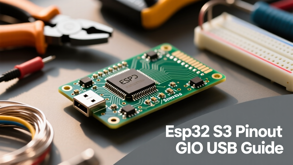
The most significant visual and architectural shift in the esp32 s3 pinout is the inclusion of native USB. This eliminates the need for external UART bridges on custom PCBs, saving BOM costs and board space.
- GPIO19 (USB_D-): The negative data line for the native USB OTG interface.
- GPIO20 (USB_D+): The positive data line for the native USB OTG interface.
When designing a custom breakout board, these pins must be routed with strict 90-ohm differential impedance controls. If you are using the ESP32-S3-DevKitC-1, these pins are already broken out to a dedicated micro-USB or Type-C connector labeled "USB".
Note: Do not confuse the native USB OTG pins with the USB Serial/JTAG interface. The JTAG interface uses GPIO26 and GPIO27 (along with GPIO19 and GPIO20 for power/ground routing in some contexts) specifically for hardware debugging and secondary serial communication. Multiplexing these pins for general I/O while expecting serial monitor output is a common beginner mistake.
Mapping the Peripherals: What You Actually Have
While the marketing materials boast 45 GPIOs, the practical reality of the esp32 s3 pinout requires careful navigation of hardware limitations. Let us break down the specific peripheral categories.
The Missing ADC2 Trap
Perhaps the most infamous quirk for makers porting legacy code to the S3 is the complete absence of ADC2. The original ESP32 featured two Analog-to-Digital Converters (ADC1 and ADC2). However, due to internal bus routing and the prioritization of Wi-Fi/Bluetooth coexistence protocols, Espressif removed ADC2 entirely from the S3 silicon.
Migration Warning: If your legacy sketch relies on
analogRead()mapped to classic ADC2 pins (like GPIO12, GPIO13, or GPIO27), your code will compile but return garbage data or zero. You must re-map all analog sensors to ADC1 channels (GPIO1 through GPIO10).
Capacitive Touch and RTC GPIOs
The ESP32-S3 features 14 capacitive touch channels, mapped to GPIO1 through GPIO14. These are highly sensitive and excellent for human-machine interfaces (HMIs) without requiring external mechanical switches. Furthermore, the S3 designates specific pins as RTC (Real-Time Clock) GPIOs. These pins remain powered during Deep Sleep modes and can be configured as wake-up sources. When designing low-power battery-operated IoT nodes, ensure your wake-up buttons or PIR sensors are routed to these specific RTC-capable pins, otherwise, the chip will not be able to rouse itself from a sub-microamp sleep state.
Critical Strapping Pins: Boot Modes and JTAG Routing
Strapping pins dictate the silicon's behavior the millisecond power is applied. If you wire a relay, a strong pull-down resistor, or an active-low sensor to a strapping pin, the ESP32-S3 will fail to boot or enter an unintended flashing mode. The Espressif Hardware Reference outlines these critical dependencies.
| GPIO Pin | Default State | Boot Behavior (Low) | Boot Behavior (High) |
|---|---|---|---|
| GPIO0 | Internal Weak Pull-Up | SPI Flash Boot (Normal) | Download Boot (Flashing Mode) |
| GPIO3 | High-Z (Floating) | Flash VDD = 3.3V | Flash VDD = 1.8V |
| GPIO45 | Internal Weak Pull-Down | Default I2C SCL / SPI Boot | Log Print via SPI |
| GPIO46 | Internal Weak Pull-Down | Default Boot Log | ROM Bootloader Log Print |
Real-World Failure Mode: Wiring a push-button to GPIO0 without a proper pull-up resistor is standard for triggering the "BOOT" button. However, if you wire an active-low relay to GPIO0 that defaults to LOW on startup, the ESP32-S3 will perpetually stall in download mode, appearing completely dead to the user.
Octal SPI and the "Lost" GPIOs on N8R8 Modules
When you purchase a popular dev board like the ESP32-S3-DevKitC-1 (N8R8 variant), it comes equipped with 8MB of Quad SPI Flash and 8MB of Octal SPI PSRAM. To support the massive bandwidth required for AI inference and audio buffering, the Octal PSRAM utilizes 8 data lines.
Because the S3 silicon has a limited pin count, Espressif routes these Octal SPI lines internally within the WROOM module package. Specifically, GPIO33 through GPIO37 are permanently consumed by the internal Octal SPI interface. If you are looking at a bare-chip pinout diagram online, you might think you have 45 usable pins. But if you are using an N8R8 module, those 5 pins are physically inaccessible on the castellation pads. Always verify your specific module's datasheet before finalizing your schematic.
Real-World Troubleshooting: Common Wiring Failures
Based on community debugging logs and the ESP32-S3 Technical Reference Manual, here are the most frequent hardware-level mistakes makers encounter when interpreting the pinout:
- I2S Microphone Routing for Edge AI: The S3 is heavily marketed for voice wake-word detection. When wiring an INMP441 I2S MEMS microphone, beginners often attempt to use the native USB pins (19/20) for I2S data. You must use standard GPIOs (e.g., GPIO4, GPIO5, GPIO6) and configure the I2S peripheral in the ESP-IDF or Arduino core to leverage the S3's DMA buffers effectively.
- SPI Camera (OV2640) Conflicts: The S3 supports 8-bit DVP camera interfaces and high-speed SPI. However, attempting to run an SD Card (SPI) and an SPI Camera simultaneously on the same SPI bus often leads to bus contention. Utilize the S3's dedicated SPI2 and SPI3 host controllers, routing the SD card to SPI2 and the Camera to SPI3 to maintain independent DMA channels.
- 5V Tolerance Myth: Like all modern 3.3V microcontrollers, the ESP32-S3 is not 5V tolerant. Feeding a 5V PWM signal from a legacy RC receiver directly into an S3 GPIO will destroy the internal ESD protection diodes and permanently short the pin to VDD. Always use a bidirectional logic level shifter or a simple voltage divider for 5V sensor integration.
Final Thoughts on Schematic Design
Mastering the esp32 s3 pinout is about understanding what the silicon cannot do just as much as what it can. By respecting the absence of ADC2, carefully managing your strapping pins, and leveraging the native USB OTG for streamlined PC communication, you can build highly capable, low-latency AI and IoT edge devices. Always cross-reference your specific WROOM module variant against the bare-chip datasheet to ensure your "available" GPIOs aren't secretly routing to internal PSRAM.