
The Prototyping Bottleneck: Decoding the ESP32 Dev Board Pinout
For hardware engineers and IoT developers, transitioning from a conceptual schematic to a working breadboard prototype should be seamless. However, the classic ESP32-WROOM-32E and its modern successors (like the ESP32-S3) introduce a unique layer of complexity. Misinterpreting the ESP32 dev board pinout doesn't just result in a non-functioning circuit; it triggers hours of phantom debugging, boot-loop mysteries, and peripheral conflicts.
As of 2026, while the ESP32 ecosystem has expanded to include the C6 and H2 variants, the foundational architecture of the original and S3 dev boards remains the industry standard for rapid prototyping. Optimizing your workflow means treating the pinout not merely as a list of available I/O, but as a strict routing matrix governed by silicon-level constraints. This guide restructures how you approach pin mapping, eliminating hardware-software conflicts before you write a single line of C++ or Rust.
Strapping Pins: Eliminating Boot-Loop Debugging
The most common workflow killer when using a new ESP32 dev board is ignoring the strapping pins. These pins are sampled by the internal bootloader during reset to determine the chip's operating mode. If your external circuit forces these pins into the wrong state, the ESP32 will either fail to flash, boot from the wrong memory bank, or output garbage to the serial monitor.
According to the official Espressif ESP32 Datasheet, there are four primary strapping pins on the classic ESP32. Integrating this table into your pre-flight hardware checklist will save hours of oscilloscope probing.
| GPIO Pin | Internal State | Logic LOW (0) Behavior | Logic HIGH (1) Behavior | Workflow Rule |
|---|---|---|---|---|
| GPIO 0 | Pull-up | Download Boot Mode (Flashing) | SPI Fast Boot (Normal) | Never tie to GND permanently; use a momentary switch. |
| GPIO 2 | Pull-down | Normal Flash Operation | Boot Failure / Flash Error | Never use for active-high outputs or pull-ups at boot. |
| GPIO 12 (MTDI) | Pull-down | Flash VDD = 3.3V (Standard) | Flash VDD = 1.8V | Leave floating or pull LOW. High = brownout on 3.3V boards. |
| GPIO 15 (MTDO) | Pull-up | Silent Boot (No logs) | Normal Boot Log Output | Pull LOW for production battery nodes to save power/EMI. |
Pro-Tip: Many off-the-shelf dev boards feature onboard LEDs tied to GPIO 2. If you attempt to use an active-high sensor on this pin during initialization, the ESP32 will refuse to enter flash mode. Always isolate onboard peripherals if they share strapping pins.
Peripheral Routing: Avoiding Hardware-Software Conflicts
The ESP32 features a highly flexible GPIO matrix, allowing you to map almost any internal peripheral to any external pin. However, relying on the GPIO matrix for every signal introduces routing delays and increases software complexity. A streamlined workflow dictates using default peripheral pins whenever possible, while strictly avoiding known silicon-level conflicts.
The ADC2 and WiFi Collision Trap
A notorious pitfall for developers building sensor nodes is the Analog-to-Digital Converter (ADC) architecture. The ESP32 features two ADC units: ADC1 and ADC2. If your project requires WiFi or Bluetooth connectivity, you cannot use ADC2. The WiFi driver hijacks the ADC2 hardware interrupt to perform RF calibration. If your code attempts to call adc2_get_raw() while WiFi is active, the ESP-IDF will silently return an ESP_ERR_INVALID_STATE error, leading to massive debugging delays.
Workflow Optimization: Exclusively route analog sensors to ADC1 pins (GPIO 32, 33, 34, 35, 36, 39). Note that GPIO 34-39 are input-only and lack internal pull-up/pull-down resistors, requiring external biasing networks for floating sensors like thermistors.
I2C and SPI Default vs. Matrix Routing
While the ESP-IDF GPIO API allows remapping I2C and SPI buses, sticking to the hardware defaults optimizes both CPU overhead and signal integrity at higher clock speeds.
- Default I2C: SDA on GPIO 21, SCL on GPIO 22. (Avoid using these for high-frequency interrupts).
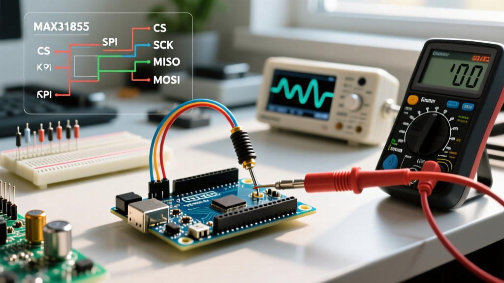
- Default SPI (VSPI): MOSI (23), MISO (19), SCK (18), CS (5).
- Default SPI (HSPI): MOSI (13), MISO (12), SCK (14), CS (15). Warning: GPIO 12 and 15 are strapping pins. Using HSPI requires careful boot-state management.
Deep Sleep & RTC GPIO Mapping Workflow
For battery-operated IoT nodes, Deep Sleep is mandatory. However, standard GPIOs lose their state and power domain when the ESP32 enters Deep Sleep. To wake the chip using an external interrupt (like a PIR sensor or a reed switch), you must route the wake signal to an RTC (Real-Time Clock) GPIO.
The classic ESP32-WROOM-32E has 18 RTC-capable GPIOs: 0, 2, 4, 12-15, 25-27, 32-39. If you accidentally route your wake-up button to a non-RTC GPIO (like GPIO 16 or 17), the chip will sleep but will never wake up, requiring a manual hardware reset. Always cross-reference your wake-up sources against the RTC domain list during the schematic capture phase.
Master Pinout Matrix for Rapid Prototyping
To accelerate your breadboard workflow, reference this optimized matrix before assigning pins in your firmware configuration file. This matrix categorizes pins by their safest and most efficient use cases, minimizing the need for mid-project rewiring.
| Category | Recommended GPIOs | Notes & Constraints |
|---|---|---|
| Safe Digital I/O | 4, 16, 17, 18, 19, 21, 22, 23, 25, 26, 27, 32, 33 | No boot-strapping conflicts. Ideal for relays, LEDs, and standard interrupts. |
| Analog Inputs (Safe) | 32, 33, 34, 35, 36, 39 | ADC1 only. Safe to use concurrently with WiFi/BT. 34-39 are input-only. |
| Capacitive Touch | 4, 12, 13, 14, 15, 27, 32, 33 | T0-T9. Requires external copper pads. Avoid routing parallel to high-speed SPI traces to prevent false triggers. |
| DAC (True Analog Out) | 25, 26 | 8-bit DAC. Excellent for generating reference voltages or simple audio waveforms without external PWM filtering. |
| UART0 (Debug) | 1 (TX), 3 (RX) | Hardwired to the USB-UART bridge on most dev boards. Do not use for secondary sensors. |
| Input-Only (No Pulls) | 34, 35, 36, 39 | Strictly inputs. Require external 10k-100k pull-up/down resistors for stable logic levels. |
From Dev Board to Custom PCB: Schematic Capture Rules
The ultimate goal of optimizing your dev board workflow is a seamless transition to a custom Printed Circuit Board (PCB). When moving from a $6 DevKit to a manufactured node, you must strip away the development-specific circuitry.
Eliminating the Auto-Reset Circuit
Standard ESP32 dev boards use a clever but component-heavy RC delay circuit involving two NPN transistors (or a dedicated IC like the CH340) to manipulate the EN (Enable) and GPIO0 pins, forcing the chip into flash mode automatically via the DTR/RTS serial lines. For a custom, cost-optimized PCB, delete this circuit. Replace it with two tactile switches: one tying EN to GND (Reset), and one tying GPIO0 to GND (Boot). This saves board space, reduces BOM costs, and eliminates phantom reset issues caused by serial noise.
Power Domain Decoupling
As highlighted in comprehensive hardware guides like Random Nerd Tutorials' ESP32 Pinout Reference, the 3V3 pin on a dev board is backed by an onboard LDO (often an AMS1117-3.3). On a custom board, you must provide your own LDO or switching buck converter. Ensure you place a 10µF bulk capacitor and a 100nF decoupling capacitor as close to the ESP32-WROOM module's VDD pin as physically possible. The RF transmission bursts can draw upwards of 500mA for milliseconds; inadequate decoupling will result in brownout resets that mimic pinout logic errors.
Summary: The Zero-Rework Philosophy
Mastering the ESP32 dev board pinout is not about memorizing 38 GPIO numbers; it is about understanding the silicon's boot sequence, peripheral domain restrictions, and power states. By treating strapping pins as immutable constraints, routing analog signals exclusively to ADC1, and respecting the RTC domain for low-power applications, you transform your hardware workflow from a cycle of trial-and-error into a predictable, zero-rework engineering process.