
When scaling an Arduino project beyond a single sensor, the Inter-Integrated Circuit (I2C) bus is the default choice for makers and engineers alike. However, as you daisy-chain OLED displays, BME280 environmental sensors, and IMUs, you will inevitably hit a wall: bus capacitance. Breadboards and long jumper wires introduce parasitic capacitance that degrades the open-drain signals, leading to corrupted data, frozen microcontrollers, and the dreaded 'shark-fin' waveform. Learning how to make an I2C pull up bus bar is the definitive hardware solution to stabilize your sensor networks.
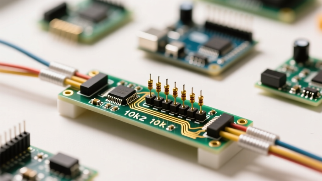
A dedicated I2C bus bar acts as a centralized hub. It consolidates power distribution, provides precise pull-up resistors, minimizes trace lengths, and offers robust physical connectors. In this comprehensive tutorial, we will cover the electrical theory, the mathematical sizing of resistors, and the physical assembly of a professional-grade I2C pull-up bus bar for your MCU projects.
The Hidden Bottleneck: I2C Capacitance and Signal Degradation
Unlike SPI or UART, I2C utilizes an open-drain (or open-collector) architecture. This means devices on the bus can only pull the SDA (data) and SCL (clock) lines LOW to ground; they cannot actively drive them HIGH. To achieve a HIGH state, the bus relies entirely on external pull-up resistors connected to the logic voltage (VCC).
Every wire, breadboard contact, and sensor pin adds a tiny amount of capacitance to the bus. According to the official NXP I2C-bus specification (UM10204), the maximum allowable bus capacitance ($C_b$) for standard-mode I2C (100 kHz) is 400 pF. When capacitance increases, the RC time constant of the pull-up resistor and the bus capacitance increases. This slows down the voltage rise time when a device releases the line. If the rise time exceeds the I2C specification limits, the Arduino's TWI (Two-Wire Interface) hardware will misinterpret the bits, resulting in I2C lockups.
Sizing Your Pull-Up Resistors: The Math Behind the Bus
You cannot simply throw a random 10kΩ resistor on the SDA and SCL lines and expect reliable operation across a complex bus bar. Sizing the pull-up resistor requires balancing two competing electrical limits: the minimum resistance (to ensure a valid LOW voltage) and the maximum resistance (to ensure a fast enough rise time).
Calculating the Minimum Resistance ($R_{min}$)
The minimum resistance is dictated by the maximum sink current ($I_{ol}$) of the devices on the bus and the maximum acceptable LOW-level output voltage ($V_{ol}$). Standard I2C devices are rated to sink up to 3 mA while maintaining a $V_{ol}$ below 0.4V.
Using Ohm's Law:
R_min = (V_cc - V_ol) / I_ol
For a 5V Arduino Uno:
R_min = (5.0V - 0.4V) / 0.003A = 1,533 Ω
Your pull-up resistors must be greater than 1.5kΩ to prevent damaging the internal MOSFETs of your sensors or MCU.
Calculating the Maximum Resistance ($R_{max}$)
The maximum resistance is constrained by the bus capacitance ($C_b$) and the required rise time ($t_r$). For standard mode (100 kHz), the maximum rise time is 1000 ns. The Texas Instruments application note SLVA704 provides the exact formula for the RC rise time between the I2C voltage thresholds:
R_max = t_r / (0.8473 * C_b)
If your bus bar and connected cables introduce 200 pF of capacitance:
R_max = 1000 ns / (0.8473 * 200 pF) = 5,901 Ω
This mathematical window reveals why 4.7kΩ is the industry standard for 5V systems with moderate capacitance. It safely sits between the 1.5kΩ minimum and the ~5.9kΩ maximum.
| Estimated Bus Capacitance ($C_b$) | I2C Speed Mode | Max Rise Time ($t_r$) | Recommended Pull-Up Resistor |
|---|---|---|---|
| < 100 pF (Short PCB traces) | Fast Mode (400 kHz) | 300 ns | 2.2 kΩ |
| 100 pF - 200 pF (Small Bus Bar) | Standard (100 kHz) | 1000 ns | 4.7 kΩ |
| 200 pF - 400 pF (Long Cables) | Standard (100 kHz) | 1000 ns | 3.3 kΩ (or Active Pull-Up) |
| > 400 pF | Requires Active Buffer | N/A | N/A (Use LTC4311 or PCA9615) |
Bill of Materials: Building the Physical Bus Bar
To construct a robust I2C pull-up bus bar, avoid cheap solderless breadboards. You need a permanent, low-capacitance physical interface. Here is the exact BOM for a professional maker's I2C hub:
- Base Substrate: FR4 Double-Sided Proto Board (0.1" pitch grid). FR4 offers lower parasitic capacitance than phenolic paper boards.
- Pull-Up Resistors: 1/4W 1% Metal Film Resistors (4.7kΩ or calculated value). Metal film offers lower thermal noise than carbon composition.
- Decoupling Capacitors: 100nF (0.1µF) MLCC Ceramic Capacitors (one for the main bus, plus optional per-port).
- Connectors: JST-PH 2.0mm right-angle connectors (for compact sensor modules) or Molex KK 2.54mm headers (for standard Arduino jumper wires).
- Power Input: 2-pin 5.08mm pitch screw terminal for main VCC and GND input.
- Bus Indicator: 2x 0805 SMD LEDs with 1kΩ current-limiting resistors (optional, for visual SDA/SCL activity monitoring).
Step-by-Step Assembly: Soldering the I2C Hub
Proper physical layout is just as critical as resistor selection. High-speed digital signals (even at 400 kHz, the harmonics extend into the MHz range) require careful routing to prevent crosstalk and ground loops.
1. Establish the Ground Plane
If using a double-sided proto board, dedicate the entire bottom copper layer to a solid ground plane. If using a single-sided board, run a thick, continuous ground trace directly beneath the SDA and SCL signal traces. This minimizes the loop area of the return currents, drastically reducing electromagnetic interference (EMI) and parasitic inductance.
2. Route the Power and Signal Rails
Run your 5V (or 3.3V) VCC rail and GND rail parallel to each other. Place the SDA and SCL traces next, but keep them separated by at least one empty row of holes from the power rails to minimize capacitive coupling. Never route SDA and SCL parallel to each other for long distances without a ground trace between them, as the clock signal (SCL) will capacitively couple into the data line (SDA), causing ghost data bits.
3. Mount and Solder the Pull-Ups
Solder the pull-up resistors as physically close to the Arduino's main input connector as possible. The pull-ups should sit at the 'root' of the bus tree. Apply a small amount of flux, tin the pads, and seat the 4.7kΩ resistors. Ensure the leads are trimmed flush to prevent sharp points that can arc or scratch enclosures.
4. Add Decoupling and Connectors
Solder the 100nF decoupling capacitor directly across the VCC and GND pins of the main screw terminal. This acts as a local energy reservoir, preventing voltage sags when multiple sensors power up simultaneously. Finally, solder your JST or Molex connectors, ensuring the pinout is standardized across all ports (e.g., Pin 1: GND, Pin 2: VCC, Pin 3: SDA, Pin 4: SCL). Standardizing the pinout prevents catastrophic reverse-polarity shorts when plugging in modules in the dark.
Expert Maker Tip: If your I2C bus bar needs to interface with both 5V Arduino Unos and 3.3V ESP32/Raspberry Pi boards, integrate a dedicated I2C level-shifter IC like the PCA9548A or a discrete N-channel MOSFET level translator (BSS138) directly onto the bus bar PCB. This isolates the 5V pull-ups from the 3.3V pull-ups, preventing overvoltage damage to sensitive 3.3V logic gates.
Debugging Signal Integrity: When the Bus Bar Fails
Even with a perfectly soldered bus bar, complex networks can fail. When your Arduino's Wire.endTransmission() returns an error code (like '2' for NACK on address), do not blindly change your code. Look at the physics.
Connect a logic analyzer (such as a Saleae Logic Pro 8 or a DreamSourceLab DSLogic Plus) to the SDA and SCL pins at the furthest sensor node from your bus bar. Trigger on the falling edge of SCL and examine the rising edge of SDA.
- The Shark-Fin Waveform: If the rising edge looks like a curved fin rather than a sharp square wave, your RC time constant is too high. The bus capacitance has exceeded the pull-up resistor's ability to charge it quickly. Solution: Decrease the pull-up resistor value (e.g., drop from 4.7kΩ to 2.2kΩ) or reduce cable length.
- Voltage Sag on LOW: If the LOW state does not reach 0V, but instead bottoms out at 0.6V or higher, a device on the bus is failing to sink the current properly, or the pull-up resistor is too strong (too low a value) for the sensor's internal MOSFET. Solution: Increase the pull-up resistance.
- Ring and Overshoot: If the signal rings (oscillates) when transitioning, you have excessive parasitic inductance, usually caused by long, unshielded ribbon cables. Solution: Twist the SDA/SCL wires with the GND wire, or add a small 33Ω series termination resistor at the MCU end of the bus bar.
Advanced Additions: Active Pull-Ups for Extreme Networks
If you are building a massive sensor array—such as a greenhouse monitoring system with 20 meters of distributed cabling—the 400 pF capacitance limit will be instantly violated. Passive resistors will fail regardless of the math.
In these scenarios, upgrade your DIY bus bar to include an Active Pull-Up IC, such as the Analog Devices LTC4311. Unlike a passive resistor, an active pull-up circuit uses a fast-switching MOSFET to forcefully drive the bus HIGH during the initial transition, then backs off to a gentle current source to prevent overshoot. This effectively eliminates the RC rise-time bottleneck, allowing you to run standard 100 kHz I2C over massive capacitances exceeding 2000 pF. Integrating an LTC4311 onto your custom FR4 bus bar transforms it from a simple breakout board into an industrial-grade signal conditioning hub.
By understanding the underlying physics of open-drain buses and taking the time to fabricate a dedicated I2C pull-up bus bar, you eliminate the most common hardware bottlenecks in Arduino prototyping. Your sensor networks will boot faster, transmit cleaner data, and survive the electrical noise of real-world environments.