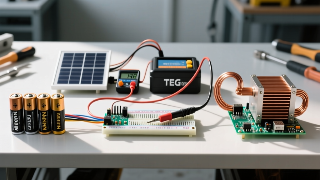

When electrical engineers, DIY hobbyists, and physics students first attempt to define electric charge in physics, they are usually met with a deceptively simple textbook answer: it is a fundamental property of matter that causes it to experience a force when placed in an electromagnetic field. However, for those of us actually building circuits, sizing wires, and programming microcontrollers, this abstract definition is practically useless. To truly master electrical fundamentals, we must move beyond rote memorization and examine charge through a comparative lens.
This guide will help you define electric charge in physics by comparing its various models, units of measurement, and transport mechanisms. By contrasting how charge behaves in a vacuum tube versus a P-type semiconductor, or how we measure it in Coulombs versus Ampere-hours, you will gain a robust, working knowledge of the invisible force that powers every DIY electronics project.
The 2019 SI Redefinition: A Fixed Constant
Before comparing how charge behaves, we must compare how it is defined at the highest metrological level. Historically, the Coulomb was defined by the physical artifacts of the Ampere (the force between two infinite parallel wires). However, in 2019, the scientific community fundamentally shifted how we define electric charge in physics.
According to the National Institute of Standards and Technology (NIST), the elementary charge e is now an exact, fixed constant of nature: 1.602 176 634 × 10⁻¹⁹ Coulombs. The Coulomb is now derived from this fixed quantum value and the definition of the second.
This shift means that charge is no longer an abstract measurement dependent on macroscopic physical experiments; it is a rigidly defined quantum baseline. This information gain is critical for high-precision electronics, where single-electron transistors and quantum computing rely on the exactitude of this fundamental constant.
Modeling Charge: Point Charge vs. Continuous Distribution
In physics and circuit design, we use two primary models to define and calculate electric charge. Comparing these two models reveals why we can use simple algebra for basic wiring but need complex calculus for high-frequency PCB trace routing.
1. The Point Charge Model (Quantum & Microscopic)
When analyzing individual electrons, protons, or isolated ions, we treat charge as a discrete point in space. This model is essential when dealing with electrostatic discharge (ESD) events, cathode ray tubes, or semiconductor doping at the atomic level. The math relies on Coulomb's Law, treating the charge as having zero physical volume but infinite local charge density.
2. The Continuous Charge Distribution (Macroscopic)
When you strip a 10 AWG THHN copper wire and look at the conductor, you are not dealing with individual electrons; you are dealing with a macroscopic sea of charge. In this model, we define electric charge in physics using volume charge density (ρ), surface charge density (σ), or linear charge density (λ). This continuous model is what allows us to use integral calculus to determine the capacitance of a coaxial cable or the electric field inside a high-voltage capacitor.
Comparing Units of Electric Charge
One of the most common stumbling blocks for DIYers is the fragmentation of charge units across different engineering disciplines. Below is a comparison chart detailing the primary units used to quantify charge.
| Unit Name | Symbol | Equivalent Value | Primary Use Case in Electronics |
|---|---|---|---|
| Coulomb | C | 1 Ampere × 1 Second | Capacitor sizing, surge protection, and fundamental physics equations. |
| Ampere-Hour | Ah | 3,600 Coulombs | Battery capacity ratings (e.g., LiPo cells for drones, 12V lead-acid for solar). |
| Milliampere-Hour | mAh | 3.6 Coulombs | Small-scale microcontroller power budgets (e.g., ESP32 IoT sensor nodes). |
| Elementary Charge | e | ~1.602 × 10⁻¹⁹ C | Quantum mechanics, semiconductor physics, and electron beam lithography. |
| Faraday Constant | F | ~96,485 Coulombs/mol | Electrochemistry, battery cell degradation analysis, and electroplating. |
Notice how the HyperPhysics database emphasizes the Coulomb for theoretical frameworks, while practical electrical engineering heavily favors the Ampere-hour. If you are designing a battery management system (BMS) for a DIY solar generator, thinking in Coulombs will only slow you down; you must translate the physics into Ampere-hours to select the correct shunt resistors and current sensors.
Charge Transport: Drift Velocity vs. Signal Propagation
A massive misconception among beginners is the speed at which electric charge moves through a wire. To properly define electric charge in physics within the context of a functioning circuit, we must compare drift velocity with signal propagation speed.
- Drift Velocity (The Physical Charge): When you apply a 12V DC potential across a 12 AWG copper wire carrying 15 Amps, the actual physical electrons are moving incredibly slowly. Using the formula v = I / (nAq), the drift velocity is approximately 0.3 millimeters per second. The physical charge carriers are practically crawling.
- Signal Propagation (The Electromagnetic Wave): Despite the slow crawl of electrons, the light bulb turns on instantly. This is because the electromagnetic field propagates through the dielectric space around the wire at a significant fraction of the speed of light (typically 60% to 90% of c, depending on the insulation's velocity factor).
Understanding this comparison is vital for high-speed digital design. When routing traces for a high-frequency microcontroller bus, you are not worrying about the physical transit time of the electrons; you are managing the propagation delay of the electromagnetic wave bouncing between the trace and the ground plane.
Charge Carriers: Electrons vs. Holes vs. Ions
When we define electric charge in physics, we often default to thinking solely of the electron. However, comparing the different types of charge carriers is essential for understanding modern electronics and electrochemistry.
Electrons (N-Type and Metallic Conductors)
In standard copper wiring and N-type semiconductors, the primary charge carriers are negatively charged electrons. They move from the negative terminal to the positive terminal (opposite to conventional current flow). In copper, these are 'free electrons' detached from the outer valence shell of the metal lattice.
Holes (P-Type Semiconductors)
In P-type silicon (used in the anodes of diodes and the source/drain of PMOS transistors), the charge carriers are 'holes'—the absence of an electron in the crystal lattice. Holes act as positively charged particles. Comparing electron mobility to hole mobility reveals a critical design constraint: electrons move roughly 2 to 3 times faster than holes in silicon. This is why NMOS transistors are inherently faster and more conductive than PMOS transistors of the exact same physical size.
Ions (Electrolytes and Plasmas)
In DIY battery building, electroplating, and neon sign transformers, charge is carried by physical ions (atoms with missing or extra electrons). Unlike the lightweight electron, an ion is massive and sluggish, which is why the internal resistance of a chemical battery increases dramatically in cold temperatures—the physical viscosity of the electrolyte impedes the heavy ionic charge carriers.
Real-World Troubleshooting: When Static Charge Attacks
Finally, we must compare dynamic charge (current flowing safely in a wire) with static charge (voltage potential waiting to arc). Electrostatic Discharge (ESD) is the ultimate enemy of the DIY electronics builder. To protect sensitive components like the ATmega328P microcontroller or high-speed MOSFETs, the industry uses specific comparison models to define charge vulnerability.
- Human Body Model (HBM): Simulates a charged human touching a component. The standard test circuit uses a 100 picofarad capacitor discharged through a 1,500-ohm resistor. Components rated for 2,000V HBM are generally safe for hand-assembly on a grounded mat.
- Charged Device Model (CDM): Simulates the component itself becoming charged (e.g., sliding down a plastic feeder tube) and discharging into a grounded metal surface. CDM events have much lower resistance (often less than 10 ohms) and result in massive, nanosecond current spikes that melt microscopic silicon interconnects.
According to guidelines published by the ESD Association, comparing the HBM and CDM thresholds of a component is mandatory before designing a consumer product. A chip might survive a 4,000V HBM strike but be destroyed by a mere 250V CDM event. Always use ionizing fans and grounded wrist straps when handling bare PCBs to neutralize static charge before it becomes a destructive dynamic current.
Summary: Synthesizing the Definition
To accurately define electric charge in physics for practical application, you cannot rely on a single sentence. You must understand it as a fixed quantum constant (the 2019 SI redefinition), a macroscopic continuous distribution (for wiring and capacitance), and a versatile entity transported by electrons, holes, or ions depending on the medium. By comparing these different facets of charge, you transition from a passive reader of textbooks to an active, deeply informed electrical designer capable of troubleshooting complex real-world failures.