
The Physics of Failure: Why Transistors Die on the Workbench
Before diving into the exact methodology of how to check transistor with multimeter tools, we must understand the physical failure modes of semiconductors. Transistors rarely fail without a reason. Bipolar Junction Transistors (BJTs) like the ubiquitous 2N3055 or 2N3904 typically succumb to secondary breakdown or thermal runaway. When a BJT exceeds its Safe Operating Area (SOA), localized hotspots form on the silicon die, melting the internal junctions and creating a permanent Collector-Emitter short.
Conversely, Power MOSFETs (such as the IRFZ44N or IRF540N) usually fail due to gate oxide punch-through or avalanche breakdown. The gate oxide layer in a MOSFET is incredibly thin—often just a few nanometers. A static discharge or a voltage spike exceeding the Gate-Source threshold (typically ±20V) will puncture this insulating layer, permanently shorting the Gate to the Source or Drain. Understanding these failure modes dictates how we interpret our multimeter readings.
Essential Multimeter Settings for Semiconductor Testing
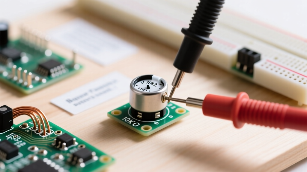
To properly test active components, you must abandon the standard resistance (Ω) mode. Resistance mode applies an unpredictable test voltage and current, which can yield wildly inconsistent readings across non-linear PN junctions. Instead, you must use the Diode Test Mode (indicated by a diode symbol on the dial).
According to Fluke's official testing guidelines, diode test mode outputs a constant current (usually between 1mA and 2mA) and measures the forward voltage drop across the component. For silicon-based BJTs, a healthy PN junction will display a forward voltage drop between 0.55V and 0.75V. Germanium transistors (now largely obsolete but found in vintage audio gear) will read between 0.20V and 0.30V. If your multimeter reads 'OL' (Open Loop), the junction is blown open. If it reads '0.00V' or near zero with a continuity beep, the junction is shorted.
Step-by-Step: Testing Bipolar Junction Transistors (BJTs)
A BJT is essentially two diodes sharing a common anode or cathode (the Base). By mapping these diodes, we can determine the health, pinout, and polarity (NPN vs. PNP) of an unmarked transistor.
Mapping NPN vs. PNP Junctions
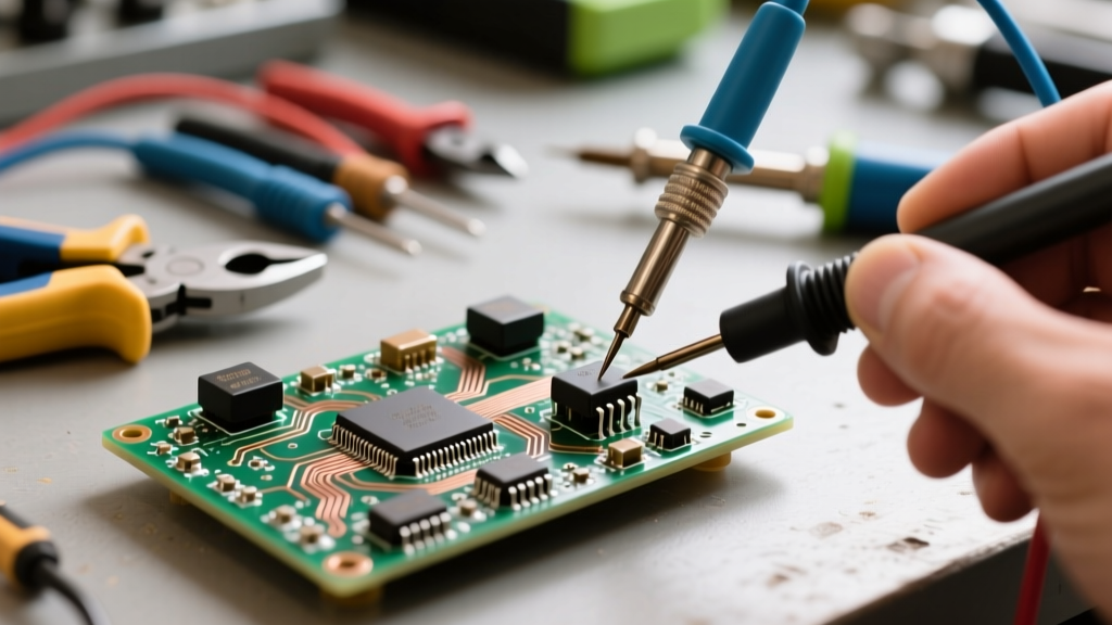
For an NPN transistor (e.g., 2N2222, BC547), the Base is the anode for both internal diodes. Place your red probe on the Base and the black probe on the Emitter. You should read ~0.65V. Move the black probe to the Collector; you should also read ~0.65V. Reversing the probes (black on Base, red on Emitter/Collector) must yield an 'OL' reading, confirming the junctions are blocking reverse voltage.
For a PNP transistor (e.g., 2N3906, BC557), the Base is the common cathode. Place your black probe on the Base and the red probe on the Emitter, then the Collector. Both should read ~0.65V. Reversing the probes must yield 'OL'.
Critical Check: Testing the Collector to Emitter directly in both directions must always result in 'OL'. If you read any voltage drop or continuity between Collector and Emitter with the Base floating, the transistor has suffered a secondary breakdown and is scrap.
The hFE Socket Trap
Many budget multimeters feature an 'hFE' socket designed to measure DC current gain. While tempting, All About Circuits warns against relying on this for fault-finding. The hFE test applies a very low test voltage and cannot detect high-voltage leakage or partial junction breakdowns. A transistor can show a 'perfect' hFE of 200 on the socket but still fail catastrophically when subjected to 30V in a switching circuit. Stick to diode mode for structural integrity testing.
Testing Power MOSFETs: Gate Charge and Body Diodes
MOSFETs require a fundamentally different approach because they are voltage-controlled devices with insulated gates. Testing an N-Channel MOSFET (like the IRF3205) involves verifying the internal body diode and the gate capacitance.
Verifying the Intrinsic Body Diode
Every standard power MOSFET has an intrinsic body diode connected between the Source and Drain, pointing from Source to Drain (for N-Channel). In diode mode, place the red probe on the Source and the black probe on the Drain. You should read a forward voltage drop between 0.40V and 0.60V. Reversing the probes (red on Drain, black on Source) must read 'OL'. If it reads 'OL' in both directions, the body diode is open. If it reads near 0V in both directions, the MOSFET is shorted.
The Gate Charge Discharge Method
To test the gate insulation and channel switching, follow this exact sequence:
- Discharge the Gate: Briefly short the Gate and Source pins with a piece of wire or your finger to drain any residual gate capacitance.
- Check Drain-Source: With the Gate discharged, measure Drain to Source (red on Drain, black on Source). It should read 'OL' because the channel is off.
- Charge the Gate: Keep the black probe on the Source. Momentarily touch the red probe to the Gate. The multimeter's internal ~2.4V test voltage will charge the gate capacitance, turning the MOSFET channel ON.
- Verify the Channel: Move the red probe back to the Drain (black remains on Source). The multimeter should now read a very low voltage drop (often 0.00V to 0.10V) or beep for continuity, proving the channel has successfully turned on.
- Discharge Again: Short Gate to Source again. The channel should turn off, returning to 'OL' when measuring Drain to Source.
ESD Warning: While the multimeter's diode test voltage is safe for most power MOSFETs, testing small-signal RF MOSFETs or ultra-sensitive logic-level devices requires a grounded wrist strap. Gate oxide punch-through can occur from static electricity on your test leads.
In-Circuit vs. Out-of-Circuit Testing Realities
A common mistake among hobbyists is attempting to check a transistor while it is fully soldered into a PCB. In-circuit testing is heavily compromised by parallel impedances. If a BJT has a 470Ω base resistor connected to VCC, your multimeter's diode test current will flow through the resistor, yielding a false reading of ~0.47V instead of the expected 0.65V junction drop.
The 1kΩ Rule: If the parallel circuitry across any two transistor pins measures less than 1kΩ on your multimeter's resistance mode, in-circuit diode testing is completely invalid. The external components will mask a shorted junction. For absolute certainty, you must desolder at least two legs of the transistor (or lift the entire component) to isolate it from the PCB traces before performing the diode test.
Troubleshooting Matrix: Multimeter Readings vs. Failure Modes
Use this reference table to quickly diagnose component health based on your multimeter's diode test readings.
| Component Type | Test Points (Red → Black) | Healthy Reading | Failure Indication | Probable Root Cause |
|---|---|---|---|---|
| NPN BJT | Base → Emitter | 0.55V - 0.75V | 0.00V (Short) | Base current overload / Thermal runaway |
| NPN BJT | Base → Collector | 0.55V - 0.75V | OL (Open) | Bond wire fracture from thermal cycling |
| NPN BJT | Collector → Emitter | OL (Both directions) | 0.00V (Short) | Secondary breakdown / Exceeded V_CEO |
| N-Ch MOSFET | Source → Drain | 0.40V - 0.60V | OL (Open) | Source bond wire lifted / Die crack |
| N-Ch MOSFET | Gate → Source | OL (Both directions) | 0.00V to 0.50V | Gate oxide punch-through (ESD / Spike) |
| N-Ch MOSFET | Drain → Source (Channel) | OL (When Gate discharged) | 0.00V (Short) | Avalanche breakdown / Overcurrent melt |
Summary Checklist for the Workbench
Mastering how to check transistor with multimeter equipment is a foundational skill for any electronics repair technician or DIY circuit designer. Always remember to use Diode Test mode, isolate the component from parallel PCB traces whenever possible, and understand the distinct architectural differences between current-driven BJTs and voltage-driven MOSFETs. By systematically mapping the PN junctions and utilizing the gate-charge trick, you can confidently sort the good silicon from the dead, saving hours of frustrating circuit debugging.