
The NE555 timer is arguably the most successful integrated circuit in the history of electronics. Invented by Hans Camenzind in 1972 for Signetics, over a billion units are still manufactured annually. Whether you are building a simple LED flasher, a precision PWM motor controller, or a debounce circuit, mastering the fundamental 555 chip schematic is a rite of passage for any electrical engineer or DIY enthusiast. This comprehensive reference and cheat sheet provides deep-dive technical insights, exact timing formulas, and professional-grade troubleshooting tips that go far beyond basic hobbyist tutorials.
Anatomy of the NE555: Internal Block Schematic & Pinout
Before wiring external components, you must understand what happens inside the silicon. The standard bipolar 555 chip schematic relies on an internal voltage divider consisting of three precise 5kΩ resistors (hence the name '555'). This divider creates two reference voltages: 1/3 VCC and 2/3 VCC. These references feed into two internal analog comparators, which in turn control an SR flip-flop. The flip-flop drives a push-pull output stage (Pin 3) and an open-collector NPN discharge transistor (Pin 7).
Standard 8-Pin DIP Pinout Reference
| Pin | Name | Function & Internal Connection |
|---|---|---|
| 1 | GND | Ground reference (0V). |
| 2 | TRIG | Trigger input. Starts timing when voltage drops below 1/3 VCC. |
| 3 | OUT | Push-pull output. Can source or sink up to 200mA. |
| 4 | RESET | Active-low reset. Forces output low if pulled below 0.7V. |
| 5 | CTRL | Control voltage. Provides access to the 2/3 VCC internal divider node. |
| 6 | THR | Threshold input. Ends timing when voltage exceeds 2/3 VCC. |
| 7 | DISCH | Discharge. Open-collector NPN transistor used to discharge timing caps. |
| 8 | VCC | Positive supply voltage (typically 4.5V to 15V for bipolar NE555). |
Core Operating Modes: The Big Three Schematics
1. Astable Mode (Free-Running Oscillator)
In an astable 555 chip schematic, the circuit continuously oscillates between high and low states without external triggering. The timing capacitor (C1) charges through resistors R1 and R2, and discharges only through R2 via the internal Pin 7 transistor. Because the capacitor must charge through both resistors but discharge through only one, the standard astable configuration cannot produce a duty cycle of 50% or lower; the high time will always exceed the low time.
Pro-Tip (The Diode Mod): To achieve a precise 50% duty cycle or lower, place a standard 1N4148 signal diode in parallel with R2. Orient the cathode (stripe) toward Pin 7. This forces the charging current to bypass R2 entirely (flowing only through R1), while the discharging current flows exclusively through R2. This decouples the high and low timing intervals, allowing for true PWM generation.
2. Monostable Mode (One-Shot Pulse Generator)
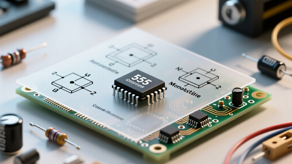
The monostable configuration outputs a single, precise pulse of a fixed duration whenever the Trigger pin (Pin 2) is momentarily pulled low (below 1/3 VCC). During the pulse, the internal discharge transistor turns off, allowing the external capacitor to charge through a single resistor. Once the capacitor voltage hits 2/3 VCC, the pulse ends and the capacitor is rapidly discharged. This schematic is ideal for switch debouncing, missing pulse detection, and timed relays.
3. Bistable Mode (Schmitt Trigger / Flip-Flop)
By omitting the timing capacitor and directly controlling the Trigger (Pin 2) and Threshold (Pin 6) pins with external switches, the 555 acts as a bistable flip-flop. Pulling Pin 2 low sets the output high; pulling Pin 6 high resets the output low. This configuration is highly effective for creating latching relay drivers or robust mechanical switch interfaces.
Component Selection & Timing Formulas Cheat Sheet
| Mode | High Time (t_high) | Low Time (t_low) | Frequency / Total Period |
|---|---|---|---|
| Astable (Standard) | 0.693 × (R1 + R2) × C | 0.693 × R2 × C | f = 1.44 / ((R1 + 2×R2) × C) |
| Monostable | t_pulse = 1.1 × R × C | N/A (Depends on trigger) | N/A (Single Shot) |
Critical Capacitor Dielectric Warnings
A frequent mistake in 555 chip schematic design is using the wrong capacitor dielectric for timing. Never use Y5V or Z5U ceramic capacitors for timing networks; their capacitance varies wildly with temperature and applied voltage. Even X7R ceramics suffer from severe DC bias voltage coefficients (a 10µF X7R cap at 12V may only exhibit 2µF of actual capacitance). For precision timing, always use C0G/NP0 ceramics (for values under 10nF) or polyester/polypropylene film capacitors for larger values. If you must use electrolytics for long delays, choose low-leakage, high-temperature (105°C) variants and account for ±20% tolerance drift.
Bypass, Decoupling, and the Crowbar Effect
The bipolar NE555 is notorious for a phenomenon known as the crowbar effect. During the transition of the output stage (Pin 3) from high to low or low to high, both the internal high-side and low-side transistors are momentarily turned on simultaneously. This creates a temporary, low-impedance short circuit directly from VCC to GND, resulting in a massive current spike that can exceed 150mA for a few nanoseconds.
If your power supply impedance is too high, this spike will cause the VCC rail to sag. Because the internal comparators reference VCC, this sag can cause false triggering, double-clocking, or erratic jitter in sensitive microcontroller circuits. To mitigate this, you must implement aggressive decoupling:
- Place a 100nF (0.1µF) X7R ceramic capacitor as physically close to the VCC (Pin 8) and GND (Pin 1) pins as possible.
- Add a 10µF to 100µF bulk electrolytic capacitor near the chip to supply the instantaneous charge required during the crowbar spike.
- Always tie the Control Voltage (Pin 5) to GND via a 10nF to 100nF capacitor to filter high-frequency noise from the internal 2/3 VCC reference node.
Common Schematic Pitfalls & Troubleshooting
Even with a theoretically perfect 555 chip schematic, real-world implementations can fail. Use this troubleshooting framework to diagnose erratic behavior:
- Output Stuck High: The Threshold pin (Pin 6) is likely floating or not reaching 2/3 VCC. Check for an open timing resistor or a leaky timing capacitor that cannot charge fully.
- Output Stuck Low: The Trigger pin (Pin 2) is being held below 1/3 VCC, or the Reset pin (Pin 4) is floating. Rule of thumb: Always tie unused Reset pins directly to VCC.
- Erratic Timing / Jitter: Usually caused by inadequate decoupling (crowbar effect) or noise injected into the Control pin (Pin 5). Ensure the 10nF bypass cap on Pin 5 is present.
- Chip Overheating: Pin 7 (Discharge) is an open-collector transistor meant only to sink current to ground. If your schematic attempts to source current from Pin 7 to charge a capacitor directly without a series resistor to VCC, you will short VCC to GND internally and destroy the chip.
Modern Alternatives: CMOS vs. Bipolar 555 Timers
While the classic bipolar NE555 is robust and cheap, modern designs often benefit from CMOS variants like the TLC555 or LMC555. According to Texas Instruments, CMOS 555 timers eliminate the crowbar current spike entirely, reducing power consumption to microamps and allowing for much smaller decoupling networks. Furthermore, CMOS timers feature rail-to-rail output swings, making them vastly superior for low-voltage (3V to 5V) battery-operated devices where the bipolar NE555's 1.5V output drop would be problematic. However, CMOS inputs have very high impedance, making them more susceptible to electrostatic discharge (ESD) and requiring careful PCB layout practices to avoid noise coupling.
For further reading on advanced timing networks and edge-case applications, the Electronics Club 555 Timer Guide and the All About Circuits Semiconductor Textbook offer excellent supplementary data on internal transistor-level behavior and non-standard oscillator topologies.